We saw previously how the MOSFET device can be interpreted as a transconductance amplifier: the input signal is \(v_{\text{GS}}\), and the output signal is \(i_D\). We can build on this concept by configuring the MOSFET in several ways to make different types of amplifiers. In all cases, we will deliberately operate the device in its saturation mode, balanced between its ON/OFF states.
MOSFETs can be arranged in a variety of configurations which can be unified into a general-purpose small-signal analysis procedure. To analyze any configuration, we only need the following information:
The ideal amplifier model is obtained by analyzing the open-circuit gain of an active-bias configuration.
The ideal output resistance is equal to the equivalent resistance looking into the corresponding terminal of the ideal active-bias configuration.
To account for the circuit’s real bias source (whether passive, PMOS, or something else), we consider the bias device to be a load resistance which forms a voltage divider at the amplifier’s output.
This general framework is suitable for analyzing all MOSFET amplifier configurations. To solve the terminal resistances, we only need two general-purpose theorems that reveal the resistance looking into the drain and source terminals.
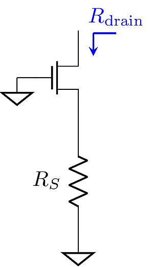
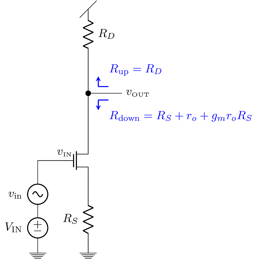
In any configuration, we can quickly solve \(R_{\rm drain}\), the equivalent small-signal resistance looking into the drain terminal of a MOSFET device. To do this, we first summarize any circuitry present under the source terminal, and treat it as a single equivalent resistance \(R_S\).
Then the circuit is reduced to the exact same model as the CS amplifier with source degeneration. We found that
\[R_{\rm drain} = R_S + r_o + g_m r_o R_S\]
This result covers all possible cases. When the source terminal is connected directly to ground, \(R_S=0\), then \(R_{\rm drain} = r_o\). If there is an ideal current source under the source terminal, then \(R_S \rightarrow \infty\), in which case \(R_{\rm drain} \rightarrow \infty\).
To find the resistance looking into the source terminal, we summarize any circuitry present above the drain as an equivalent resistance, \(R_D\).
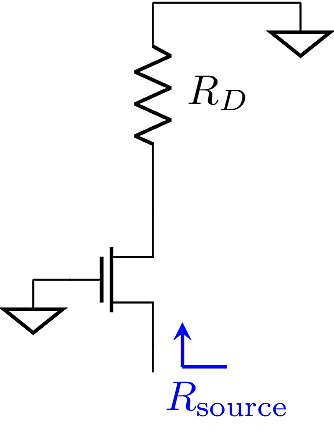

We then apply a test voltage at the source and solve for the current that flows into the source terminal:
\[\begin{aligned} i_s &= \frac{v_d}{R_D}\\ v_d &= v_s + r_o\left(g_m v_s - i_s\right)\\ \Rightarrow i_s \left(R_D + r_o\right)&= v_s\left(1+g_m r_o\right) \\ \Rightarrow R_{\rm source} = \frac{v_s}{i_s} &= \frac{R_D + r_o}{1 + g_m r_o}.\end{aligned}\]
In the coming sections we will apply these general principles to an expanding array of configurations.
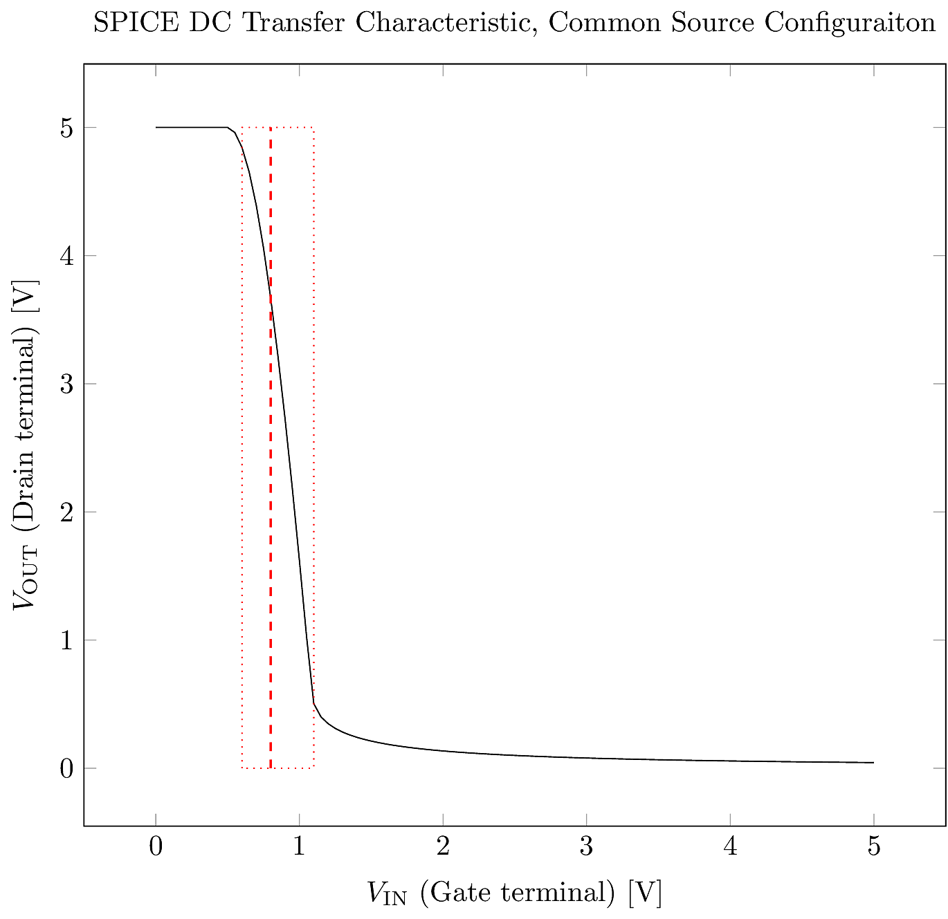
As a first example, we consider the NMOS RTL inverter circuit, only now we will try and balance the circuit at the point where its transfer characteristic is steepest. We refer to this as the bias point, or DC operating point. We then superimpose a small AC signal on top of the DC operating point. Amplifier design is therefore divided into two tasks: biasing and small-signal analysis. We’ll consider biasing strategies later. In this section we focus on basic small-signal analysis techniques, as they dictate amplifier behavior and potential applications.
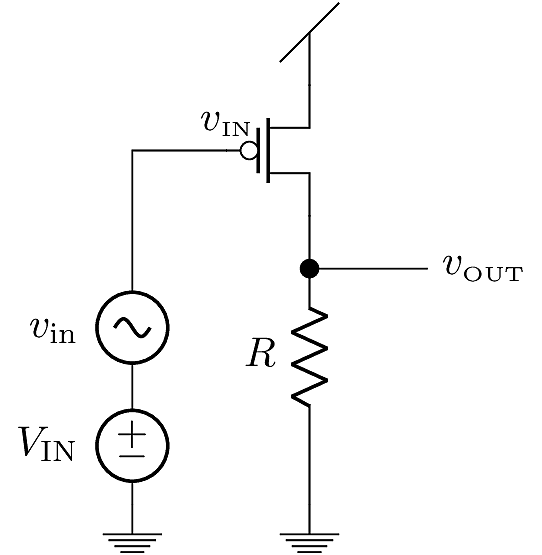
To begin with, we consider the common-source configuration and assume it is appropriately biased at a suitable DC operating point. To analyze the small-signal behavior, we replace the MOSFET with its small-signal equivalent model (the transconductance amplifier model). Second, we zero-out any DC independent sources. This means that the \(V_{\text{DD}}\) node gets shorted to ground, so any devices connected to it are “folded over” onto the ground node.


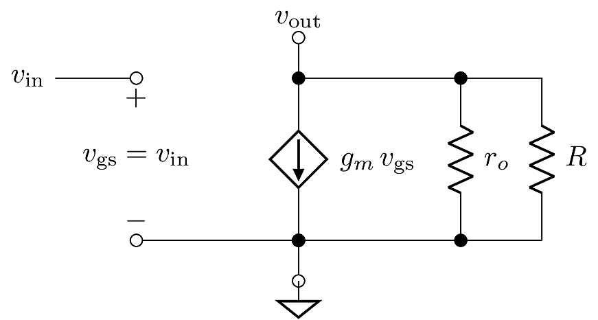
To analyze the amplifier characteristics, we use the small-signal equivalent circuit to solve for the gain and output resistance. From the small-signal model, we see that the amplifier consists of a current source and two resistors. Since the two resistors appear in parallel, we can merge them as \(R_o^\prime = r_o \parallel R\). Then the output voltage is simply the voltage drop across \(R_o^\prime\). Since the current is drawn upward through \(R_o^\prime\), the voltage drop is negative. Solving for the gain:
\[\begin{aligned} v_{\text{out}}&= -\left(g_m\,v_{\text{in}}\right)\,R_o^\prime\\ \Rightarrow A_v = \frac{v_{\text{out}}}{v_{\text{in}}} &= -g_m\,R_o^\prime\end{aligned}\]
To solve the output resistance, we set the input signal to zero and solve for the equivalent resistance seen looking into the output node. Since there is a literal resistance of \(R_o^\prime\) at that node, the output resistance is clearly \(R_o^\prime\).
Now let’s consider the complementary PMOS version of the common-source circuit. This circuit is obtained by swapping the vertical positions of the MOSFET and resistor. In the PMOS device, the drain current has an inverse response to the gate voltage: when \(v_\text{IN}\) rises, \(i_D\) falls. Since the resistor is positioned between the drain and ground, a smaller current means a smaller output voltage at the drain. The result is that the small-signal behavior is the same for both the NMOS and PMOS versions.
To obtain the small-signal equivalent circuit, we zero-out \(V_{\text{DD}}\) and \(V_{\text{IN}}\), so that the PMOS source terminal is connected to small-signal ground. Even though the PMOS device current has an inverse response to the gate voltage, we can flip the device upside down so that the source terminal is folded back onto the ground node. We then obtain the exact same model as we had for the NMOS version. What this means is that every NMOS circuit configuration should have a complementary PMOS version with the exact same behavior. The only differences will be in the device’s \(k\), \({V_{\text{Th}}}\) and \(\lambda\) parameters.
In the previous examples, we considered CS amplifiers where MOSFET is coupled with a resistor. It is often more useful to consider the active bias configuration, where the resistor is replaced by an ideal current source. This removes \(R\) from the small-signal model. Since the bias current is forced by an ideal DC independent current source, in the small-signal model contains an open-circuit at the MOSFET’s drain node. As a result, this configuration achieves the highest possible gain magnitude for a given MOSFET device.

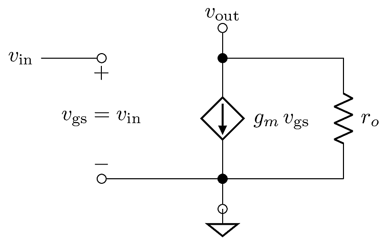
The gain and output resistance are
\[\begin{aligned} A_{vo}&= -g_m\,r_o\\ R_{\text{out}}&= r_o\end{aligned}\]
The gain magnitude of this configuration, \(g_m\,r_o\), is commonly referred to as the intrinsic gain of the MOSFET, since it is the highest gain achievable with a single MOSFET device. When the circuit is analyzed with no load attached, it is referred to as the open-circuit gain and the subscript letter ‘o’ is added in \(A_{vo}\) to signify this.
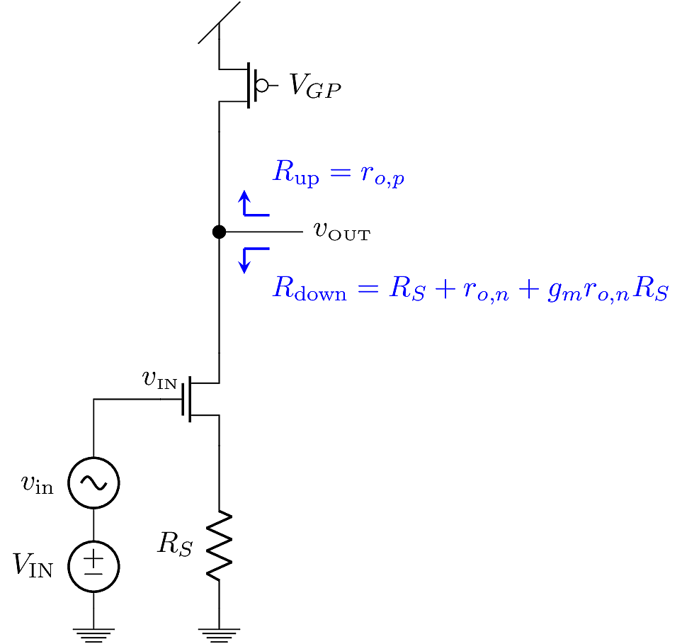
In practice, a nearly-ideal current source can be implemented using a MOSFET device with a constant gate voltage. For example, a PMOS device can be substituted in place of the current source. The PMOS gate voltage, \(V_{GP}\), should be chosen so that the device is biased in its saturation mode. In that configuration, the PMOS device is insensitive to the voltage at its drain terminal, so its constant gate voltage maintains a constant bias current \(I_D\).
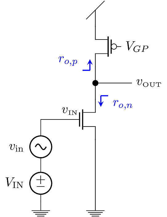
Since the PMOS device is not perfectly ideal, it contributes a load effect due to its intrinsic resistance \(r_o\). In the small-signal model, the NMOS and PMOS \(r_o\)’s will appear in parallel, so the output resistance and gain are slightly modified:
\[\begin{aligned} R_{\text{out}}&= r_{o,n} \parallel r_{o,p}\\ A_v &= -g_m\, R_{\text{out}}\end{aligned}\]
By using a PMOS device the circuit’s gain is roughly cut in half due to the interaction of \(r_o\)’s. In general, an amplifier’s output node is connected to two branches, one “going up” toward \(V_{\text{DD}}\) and another “going down” toward ground. The total output resistance is taken as the parallel combination of equivalent resistance looking up with the resistance looking down, i.e. \(R_{\text{out}}= R_{\rm up}\parallel R_{\rm down}\).
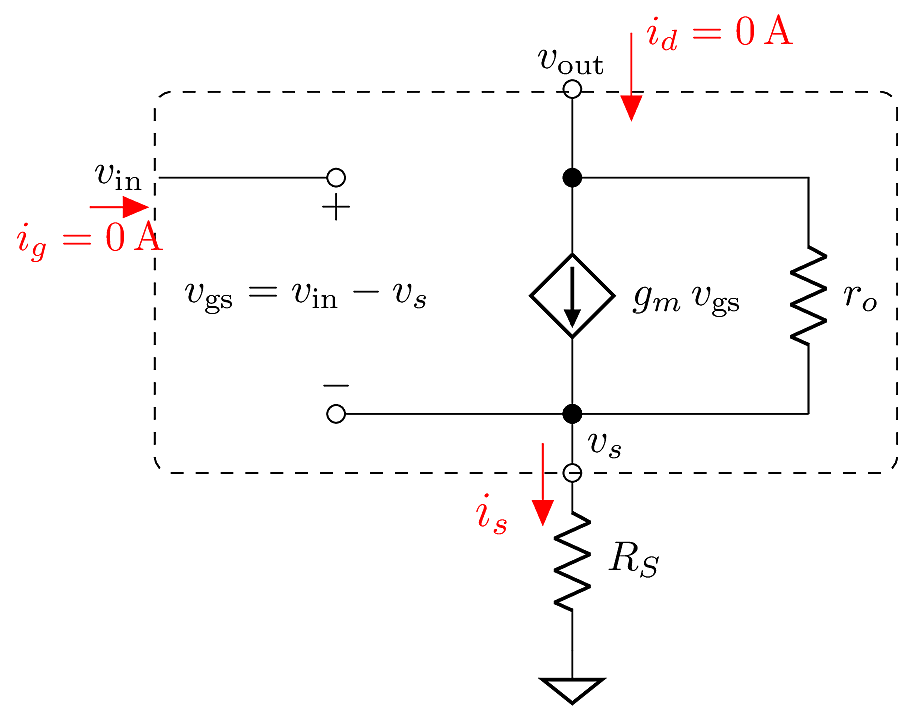
The active-bias CS amplifier is extremely sensitive to its bias point. If the DC gate voltage is off by a small error, then the circuit is easily driven to its rail voltages and rendered useless. In order to relax the bias sensitivity, we can insert a degeneration resistor under the source terminal.

 )
)
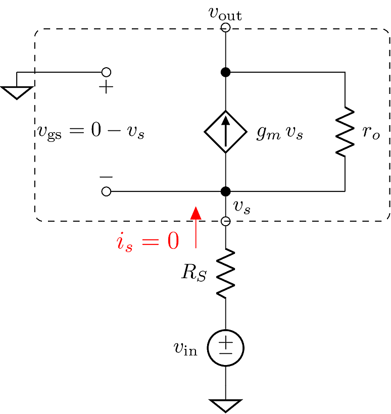
To solve the gain for this configuration, we first observe that the output node is open-circuited in the small-signal equivalent circuit model, since DC bias current source was zeroed out. In that case, the current flowing into the output branch must be zero. If a portion of the circuit is enclosed by the dashed box shown in the small-signal model, then the total current flowing into the box has to equal the total current flowing out of the box (this is a version of Kirchoff’s current law). The MOSFET does not allow any current at its gate terminal, so the gate current is zero. The output terminal is open-circuited, so the drain current is also zero. The only remaining branch is the source terminal, which must be zero since there is no other route for current to flow into the box. Since \(i_s=0\), there is no voltage drop across \(R_S\), so the source voltage is also zero.
As a result of this analysis, the model for solving the gain of this circuit is identical to the model with no degeneration, so the gain must be exactly the same, \(A_v = -g_m\,r_o\). Where the models differ is in the output resistance. To find \(R_{\text{out}}\) for this circuit, we zero out the input signal and apply a test voltage at \(v_{\text{out}}\). Then we solve for the current that flows through the output branch. Since the output node is no longer open-circuited, a non-zero current flows through the drain and source terminals, with \(i_d = i_s = i_{\rm out}\). Also, since \(v_{\text{in}}=0\), the gate-source voltage is \(v_{\text{gs}}=-v_s=-i_s\,R_S\). Based on these considerations, we obtain the circuit shown in the model below.
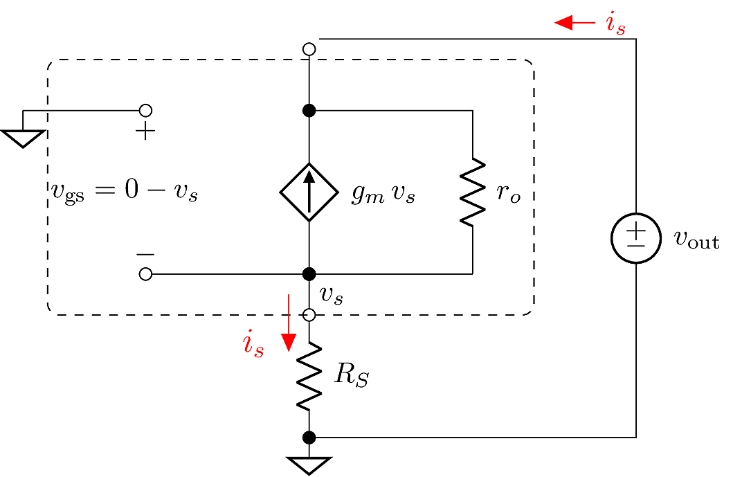
To solve for the output resistance, we consider the voltage drop across \(r_o\). Two downward currents are superimposed on \(r_o\):
\[\begin{aligned} v_{\text{out}}&= v_s + r_o\left(g_m\,v_s + i_s\right)\\ &= i_s\,R_S + r_o\left(g_m\,i_s\,R_S + i_s\right)\\ \Rightarrow R_{\text{out}}= \frac{v_{\text{out}}}{i_s} &= R_S + r_o + g_m\,r_o\,R_S\end{aligned}\]
So although the active-bias open-circuit gain is the same when source degeneration is present, the output resistance is much higher. This should result in a more significant coupling effect when a load is connected.
In the passive-bias configuration, we can leverage our previous analyses to solve the small-signal behavior without repeating the entire process. This circuit can be viewed as a superposition of the active-bias open-circuit configuration with the bias resistor \(R_D\) applied as a load:
The gain can be considered as the loaded-gain of the active-bias version:
\[\begin{aligned} A_{vL} &= \left(-g_m\,r_o\right)\frac{R_D}{R_D+R_{\text{out}}}\\ &= \frac{-g_m r_o R_D}{R_D + R_S + r_o + g_m r_o R_S}\end{aligned}\]
Another way of looking at it is that the resistance \(R_D\) summarizes the circuit’s “up” branch, and the open-circuit amplifier summarizes the circuit’s “down” branch. The two branches can be analyzed separately, and then joined together via a coupling analysis. After coupling, the new overall output resistance is \(R_{\text{out}}^{\prime} = R_{\text{out}}\parallel R_D\).
When a PMOS device is used to supply the amplifier’s active bias current, we can adopt the same approach as in the passive case. We now consider the amplifier to be loaded by the \(r_o\) of the PMOS device:
\[\begin{aligned} A_{vL} &= \left(-g_m\,r_{o,n}\right)\frac{r_{o,p}}{r_{o,p}+R_{\text{out}}}\\ &= \frac{-g_m r_{o,n} r_{o,p}}{R_S + r_{o,n}+r_{o,p} + g_m r_{o,n} R_S}\end{aligned}\]
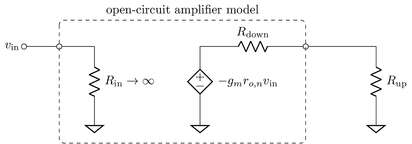
In both the passive and PMOS biased circuits, we make use of the idealized amplifier model shown below.
From the preceding analysis, it sounds like source degeneration is purely harmful, since it significantly reduces the gain. There are three good reasons for understanding source degeneration:
It is sometimes an unavoidable feature of some circuits.
It models the coupling behavior when multiple MOSFET amplifiers are folded together into a complex circuit.
It provides a looser error tolerance for biasing the common-source
Of these reasons, the third point is the most practical consideration at this stage in our study of MOSFET amplifiers. A high-gain CS amplifier can be difficult to successfully bias in practice. Since the transfer characteristic is very steep, a slight error can cause the amplifier to rail, making it useless. By inserting a degeneration resistor, we can flatten the transfer characteristic and make it more tolerant to bias error.
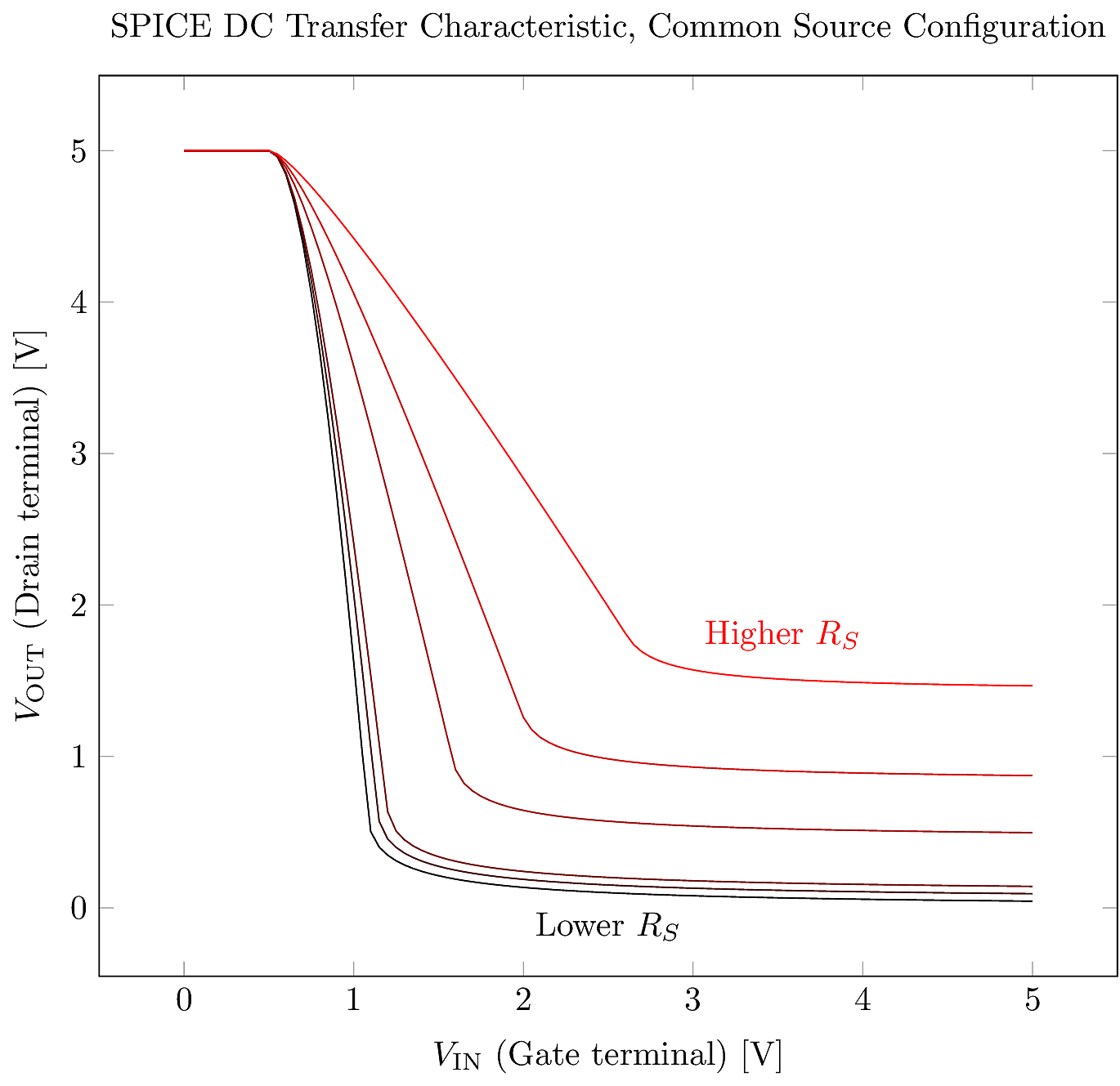
A collection of simulated DC transfer characteristics is shown in the figure below. The degeneration resistance is varied from zero up to \(20\,{\text{k}\Omega}\). With increasing values of \(R_S\), two drawbacks are visible. First, the gain is diminished, which is evident from the flatter slope in curves with higher \(R_S\). Second, the output signal range is diminished, since the transfer characteristic flattens out at a higher voltage. This limits the minimum output voltage that can appear, so we can’t produce a full \(5\,{\text{V}}\) rail-to-rail signal in this example.
For applications where only high-frequency signals need to be amplified, a win-win solution is possible by inserting a bypass capacitor across the degeneration resistor. The bypass resistor has the effect of shorting out \(R_S\) when processing high-frequency signals. But at DC, the capacitor has no effect on the circuit.
At a given frequency \(f\), the bypass capacitor \(C_B\) behaves approximately like a resistance of magnitude \((2\pi f C_B)^{-1}\). At higher frequencies this resistance tends toward zero, hence “bypassing” \(R_S\). The amplifier’s gain will then tend toward the loaded gain without degeneration:
\[A_{vL} \rightarrow -g_m r_o \left(\frac{R_D}{R_D + r_o}\right).\]

If the input signal is applied to the gate while the output is sampled from the source terminal, the circuit is called a common-drain configuration, more popularly known as a source follower since the source terminal “follows” the gate signal with a small-signal gain close to one.
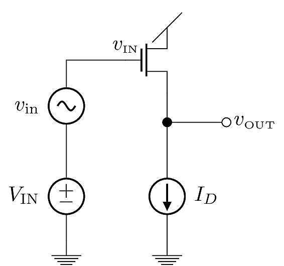
In the ideal source follower, the DC bias current is defined by an independent DC current source:

For the ideal active-biased open-circuit configuration, the small-signal model is quite simple. We see immediately that \(v_{\text{out}}= g_mr_o\left(v_{\text{in}}-v_{\text{out}}\right)\), so the open-circuit gain is simply
\[A_{vo} = \frac{g_m r_o}{1 + g_m r_o}.\]
The output resistance is a little more subtle. Since the resistance is looking into the source terminal, we should have \(R_{\text{out}}= R_{\rm source}\) with \(R_D=0\). Then
\[R_{\text{out}}= \frac{r_o}{1+g_mr_o} \approx \frac{1}{g_m}.\]
The \(1/g_m\) approximation is accurate when \(g_m r_o \gg 1\), which is usually true.
If a resistor \(R_S\) is used instead of the ideal current source, we can treat it as a load applied to the ideal open-circuit configuration. Then the loaded gain is
\[\begin{aligned} A_{vL} &= \frac{g_m r_o}{1 + g_m r_o} \frac{g_m R_S}{1+ g_mR_S}\\ &\approx \frac{g_m R_S}{1 + g_m R_S}\end{aligned}\]
This approximation applies when \(g_m r_o \gg g_m R_S\), which is often the case when using a passive bias. Finally the output resistance is
\[R_{\text{out}}= \frac{1}{g_m} \parallel R_S.\]
This tends to be much lower than the output resistance of the CG and CS configurations. For that reason, the SF configuration can be useful as an output buffer to drive small-resistance loads without suffering signal attenuation due to output resistance coupling.
In the common-gate (CG) configuration, the input signal is applied to the source terminal, the output is sampled from the drain terminal, while the gate terminal is held at a constant bias voltage.
The most ideal common-gate configuration uses an independent DC current source to define the DC bias current. The gate voltage is adjusted to a constant value such that the device’s saturation current precisely matches the DC bias current.

In the small-signal equivalent model, the gate voltage is zeroed-out to small-signal ground, and the bias current source is zeroed-out so that it becomes an open-circuit. Since no current flows out of the open-circuited drain terminal, there must also be no current flowing through \(R_S\), i.e. \(i_s=0\). Therefore \(v_s=v_{\text{in}}\). Then \(v_{\text{out}}\) is determined by the voltage drop across \(r_o\):
\[\begin{aligned} v_{\text{out}}&= v_{\text{in}}+ g_mr_o v_{\text{in}}\\ \Rightarrow A_{vo} = \frac{v_{\text{out}}}{v_{\text{in}}} &= 1+g_m r_o.\end{aligned}\]
The output resistance for this configuration is the resistance looking into the drain, which we already know is:
\[R_{\text{out}}= R_{\rm drain} = R_S + r_o + g_m r_o R_S.\]
The input resistance is the resistance seen looking into the source terminal. Since there is an ideal current source connected above the drain, the effective resistance above the drain is \(R_d\rightarrow\infty\), so for this configuration,
\[R_{\text{in}}=R_{\rm source} = \infty.\]
If the \(I_D\) current source is replaced by a resistor \(R_D\), we can consider \(R_D\) as a load resistance. Then the amplifier’s gain is revised by considering the coupling ratio:
\[A_{vL} = \left(1+g_m r_o\right) \frac{R_D}{R_D + R_S + r_o + g_m r_o R_S}.\]
When the CG amplifier is used to amplify AC signals, we can use a procedure similar to the bypass method that we applied in the CS amplifier with source degeneration. In this configuration we can similarly leverage \(R_S\) to provide a more tolerant bias point at DC, while bypassing \(R_S\) to mask its effect at higher frequencies.

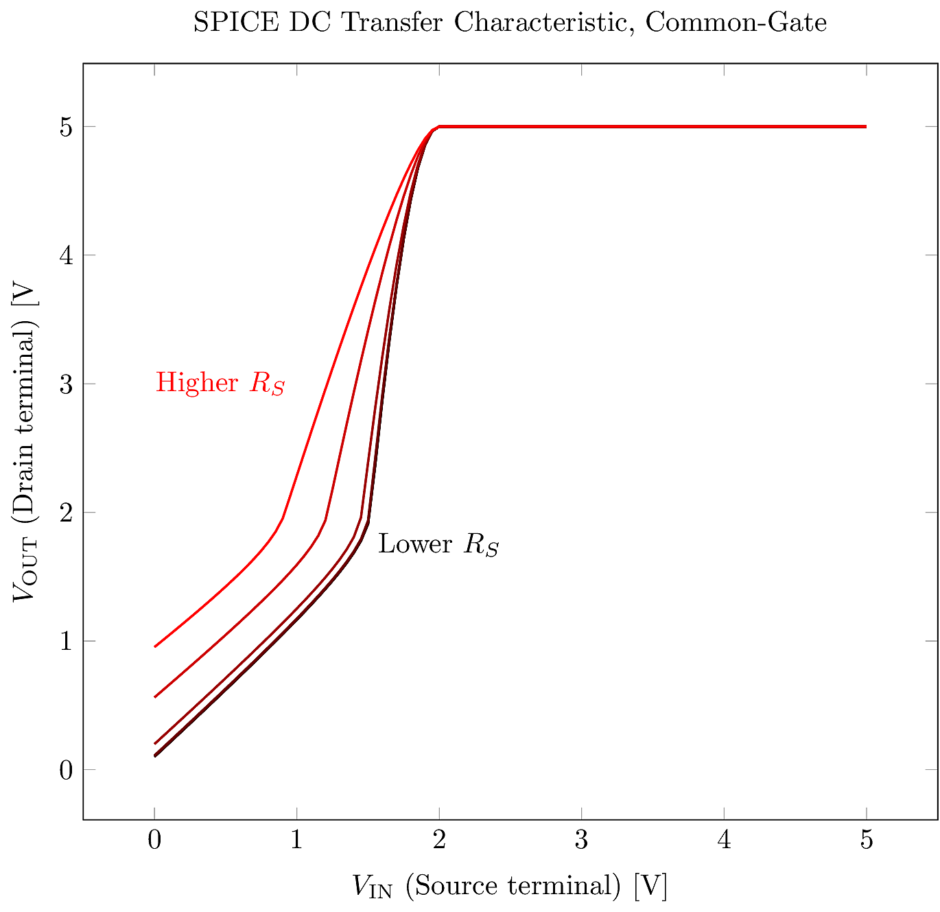
An ensemble of DC transfer characteristics are shown in the simulation plot above. The steepest curve corresponds to an \(R_S\) near zero. The steepest curve offers the best gain, but the flattest curve offers the most tolerant bias point. By using capacitive coupling, the circuit will “see” the flatter high-\(R_S\) curve at DC, but will “see” the steeper low-\(R_S\) curve at high frequencies.
In some applications, we are specifically interested in the input resistance coupling for the passive-bias configuration. The CG input resistance is defined as the resistance looking into the source terminal, \(R_{\rm source}\), which depends on the value of \(R_D\) together with any load resistance that might be present. This creates a tricky situation: we can either account for \(R_D\) via the input coupling OR account for it via the output coupling. If we model input and output coupling effects at the same time, \(R_D\) is double-counted.
In our previous output-side analysis, we considered the open-circuit analysis and later inserted \(R_D\) as a load. In the input-side analysis, we consider the short-circuit configuration with \(R_S\) removed, then insert it as a coupling resistance on the front side. In that case, the solution changes a little:
\[\begin{aligned} R_{\text{in}}&= \frac{R_D + r_o}{1+g_m r_o}\\ R_{\text{out}}&= R_D \parallel r_o\\ A_{vs} &= \frac{R_D}{R_D+r_o}+ g_m \left(R_D \parallel r_o\right)\\ A_{vL} &= \left(\frac{R_D}{R_D+r_o}+ g_m \left(R_D \parallel r_o\right)\right) \frac{R_{\text{in}}}{R_{\text{in}}+ R_S}\\ &= \frac{\left(\frac{R_D}{R_D+r_o}+g_m\frac{R_D r_o}{R_D+r_o}\right)\left(R_D+r_o\right)}{\left(1+g_mr_o\right)\left(\frac{R_D + r_o}{1+g_m r_o} + R_S\right)}\\ &= \frac{R_D+g_mR_D r_o}{R_D + r_o+ R_S+g_m r_o R_S}\\ &= \left(1+g_m r_o\right)\frac{R_D}{R_D + r_o+ R_S+g_m r_o R_S}\end{aligned}\]
The same result we obtained before.