
ECE 3410/5420

Diodes can perform logic operations, but they cannot perform:
NOT, NAND or NOR operations – diode logic gates are not universal!
Amplification – signals attenuate as they pass through diode networks, so large-scale systems are impossible with diodes alone.
Amplification is the fundamental characteristic needed for logic circuits – the device must be able to deliver more energy at its output than provided at its input.

The MOSFET has three terminals, source, gate and drain. We may first understand the MOSFET as a logic switch. In this model, the terminal potentials are interpreted as logic values, i.e.the logic set \(\left\{0,\,1\right\}\) is mapped to the potential values \(\left\{0,\,V_{\rm DD} \right\}\). Under this model we may consider all signals to be either HIGH or LOW. Then the behavior is as follows:
| Device Type | \(v_G\) | Device State | \(v_{DS}\) |
|---|---|---|---|
| NMOS | HIGH | ON | small |
| LOW | OFF | large | |
| PMOS | HIGH | OFF | large |
| LOW | ON | small |
Notice two things:
The NMOS and PMOS have complementary behavior, i.e. they have opposite states in response to the gate voltage.
When the device is ON, the drain-source voltage \(v_{DS}\) must be quite small. When the device is OFF, the drain-source voltage can be large. This is (roughly) the behavior we expect from a switch.
The MOSFET is an analog device, meaning it does not merely have “OFF” and “ON” states, but has a continuous range of in-between states. If a MOSFET is balanced in an “almost-on” state, known as its saturation mode, it produces an approximately constant current. Therefore we can use a MOSFET device to implement a DC current source.
In practice, an NMOS device first begins to switch ON when its \(V_{\text{GS}}\) crosses a device-specific threshold voltage, \({V_{\text{Th}}}\). When \(V_{\text{GS}}\) is just slightly above \({V_{\text{Th}}}\), the device enters its saturation mode. If \(V_{\text{GS}}\) is increased, the current increases. If \(V_{\text{GS}}\) is held constant, the current stays constant. If we keep increasing \(V_{\text{GS}}\), the device eventually turns fully ON, at which point it no longer acts like a current source, and behaves more like a small resistor.
In the PMOS case, the device first begins to switch ON when its \(V_{SG}\) voltage exceeds the device’s \({V_{\text{Th}}}\), which places the device in its saturation mode. The behavior is again complementary to the NMOS: as \(V_G\) is lowered, \(V_{SG}\) increases, and the current increases. Eventually, when \(V_G\) becomes low enough, the PMOS device turns fully ON and no longer works like a current source.
If the MOSFET is balanced in its saturation mode, and a time-varying signal is applied to the gate, the device’s current will change in response to the gate signal. Hence the MOSFET in saturation is considered to be a transconductance amplifier: it produces a current output (at the drain) in response to a voltage input (at the gate).
One of our key design tasks will be to balance the MOSFET in the appropriate mode for our intended application. When making switching circuits, we want the MOSFET to be toggle between ON and OFF states. When making a current source or an amplifier, we want the MOSFET to be suspended in between, in its saturation mode, with a relatively small value of \(V_{\text{GS}}\) (for NMOS) or \(V_{SG}\) (for PMOS).
The MOSFET is of course more complicated than the switch model implies. To get a more detailed picture of MOSFET behavior, we may consider an alternative invterter circuit known as the resistor-transistor logic (RTL) configuration. The RTL circuit is inferior to the CMOS configuration in that it draws static power when the NMOS device is ON. This is because the MOSFET must pull a constant current through the resistor \(R\) in order to maintain a low output voltage. It is nevertheless helpful to study the RTL inverter, because its properties are somewhat easier to analyze than the CMOS design.


The RTL inverter’s DC transfer characteristic is split into three regions, representing the different modes of the NMOS device:
Cutoff— When \(v_\text{IN}\) is below the devices threshold, \({V_{\text{Th}}}\), it is considered OFF and behaves like an open circuit between the Drain and Source.
Saturation — When \(v_\text{IN}\) is slightly greater than \({V_{\text{Th}}}\), the device is partially turned ON. The output voltage is determined by the current through the MOSFET, which depends strongly on \(v_\text{IN}\).
Triode — The device is considered fully ON when \(v_\text{OUT}< v_\text{IN}- {V_{\text{Th}}}\). In this mode, the Drain and Source are almost short-circuited.
The precise behavior of a MOSFET device is modeled by three different equations corresponding to three operating modes. The equations are qualitatively different, but they should be piecewise continuous (i.e. they should connect at the boundaries between each mode). These equations relate the device’s drain current, \(i_\text{DS}\), to the gate-source and drain-source voltages \(v_{\text{GS}}\) and \(v_{\text{DS}}\), respectively. To simplify the equations, we define the Overdrive Voltage as
\[v_{\text{OV}}\triangleq \left|v_{\text{GS}}\right| - \left|{V_{\text{Th}}}\right|.\]
Then the device equations are:
Cutoff — \(v_{\text{OV}}\leq 0\): \[i_\text{DS}= 0\]
Saturation — \(v_{\text{OV}}> 0\) and \(\left|v_{\text{DS}}\right| > v_{\text{OV}}\): \[i_\text{DS}= \frac{1}{2}kv_{\text{OV}}^2.\]
Triode — \(v_{\text{OV}}> 0\) and \(\left|v_{\text{DS}}\right| \leq v_{\text{OV}}\): \[i_\text{DS}= k\left(v_{\text{OV}}\left|v_{\text{DS}}\right| - \frac{1}{2}\left|v_{\text{DS}}\right|^2\right).\]
In these equations, \(k\) is a scale constant with units \(\mu\)A/V\(^2\), and is typically on the order of 100\(\,{\mu \text{A} / \text{V}^2 }\) to 1\(\,{\text{mA} / \text{V}^2 }\). The threshold voltage is a manufacturing parameter that varies widely between different technologies. It is typically between 0.4\(\,\text{V}\) and 2\(\,\text{V}\).
Considering the NMOS RTL inverter shown above, suppose \({V_{\text{Th}}}=2\,\text{V}\), \(k=100\,{\mu \text{A} / \text{V}^2 }\), \(R=100\,{\text{k}\Omega}\) and \(V_{\text{DD}}=5{\text{V}}\). Given the model equations above, solve for the DC transfer characteristic of \(v_\text{OUT}\) as a function of \(v_\text{IN}\).
Solution: We may divide the analysis into the three regions, and determine the points where these regions meet. Since the MOSFET’s source terminal is tied to ground, we observe that \(v_{\text{GS}}=v_\text{IN}\) and \(v_{\text{DS}}=v_\text{OUT}\). If we imagine that \(v_\text{IN}\) is initially zero, and is slowly increased toward \(V_{\text{DD}}\), then we have three subproblems:
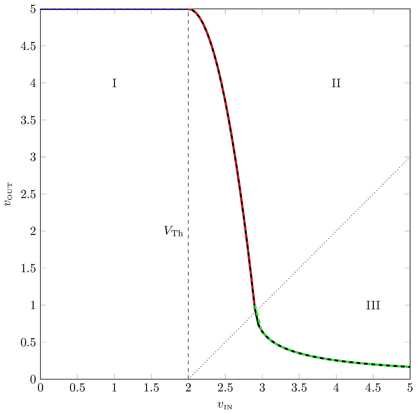
Cutoff— When \(v_\text{IN}< {V_{\text{Th}}}\), verify that \(v_{\text{OV}}<0\), therefore \(i_\text{DS}=0\). In that case, there is no current flowing through \(R\), so \(v_\text{OUT}=V_{\text{DD}}=5\,{\text{V}}\).
Saturation — When \(v_\text{IN}>{V_{\text{Th}}}\), then \(v_{\text{OV}}>0\) and the device’s current is given by the square-law equation. Then \(v_{\text{out}}\) is determined by the voltage drop across \(R\): \[\begin{aligned} v_\text{OUT}&= V_{\text{DD}}- \frac{1}{2}Rkv_{\text{OV}}^2\\ &= 5\,{\text{V}}- 5\left(v_\text{IN}-2\,{\text{V}}\right)^2 \end{aligned}\] As \(v_\text{IN}\) increases, \(v_\text{OUT}\) will decrease until the MOSFET enters the triode mode. That transition happens when \(v_\text{OUT}=v_{\text{OV}}\), i.e. \[\begin{aligned} v_{\text{OV}}&= 5\,{\text{V}}- \frac{1}{2}Rkv_{\text{OV}}^2\\ \Rightarrow 0 &= \frac{1}{2}Rkv_{\text{OV}}^2 + v_{\text{OV}}- 5 \end{aligned}\] Since the result is a quadratic equation, we can apply the standard formula and solve: \[\begin{aligned} v_{\text{OV}}&= \frac{-1 \pm \sqrt{\left(1\right)^2 - 4\left(\frac{1}{2}Rk\right)\left(-V_{\text{DD}}\right)}}{Rk}\\ &= \frac{-1 \pm \sqrt{1+2RkV_{\text{DD}}}}{Rk}\\ \textrm{if~}2Rk \gg 1:~v_{\text{OV}}&\approx \sqrt{\frac{2V_{\text{DD}}}{Rk}} \end{aligned}\] Note that we chose the positive result in the quadratic equation, since \(v_{\text{OV}}\) has to be positive in both saturation and triode, otherwise these equations wouldn’t apply. The results are: \[\begin{aligned} \textrm{exact:~} v_{\text{OV}}&= 0.905\,{\text{V}}\\ \textrm{approx:~} v_{\text{OV}}&\approx 1\,{\text{V}} \end{aligned}\] And the corresponding values of \(v_\text{IN}\) are: \[\begin{aligned} \textrm{exact:~} v_\text{IN}&= 2.905\,{\text{V}}\\ \textrm{approx:~} v_\text{IN}&\approx 3\,{\text{V}} \end{aligned}\]
Triode — When \(v_\text{IN}>2.5188\,{\text{V}}\), the device should enter triode, and the new device equation is \[\begin{aligned} i_\text{DS}&= k\left(v_{\text{OV}}v_\text{OUT}- \frac{1}{2}v_\text{OUT}^2\right)\\ \Rightarrow v_\text{OUT}&= V_{\text{DD}}- Rk\left(v_{\text{OV}}v_\text{OUT}- \frac{1}{2}v_\text{OUT}^2\right) \end{aligned}\]
Once again we can arrange this in the form of a quadratic equation: \[\begin{aligned} 0 &= \frac{1}{2}Rkv_\text{OUT}^2 - \left(1+Rkv_{\text{OV}}\right)v_\text{OUT}+ V_{\text{DD}}\\ v_\text{OUT}&= \frac{\left(1+Rkv_{\text{OV}}\right) \pm \sqrt{\left(1+Rkv_{\text{OV}}\right)^2 - 2RkV_{\text{DD}}}}{Rk}\\ &= \frac{\left(1+Rkv_{\text{OV}}\right) - \sqrt{1+\left(Rkv_{\text{OV}}\right)^2}}{Rk} \end{aligned}\] Note that if \(Rkv_{\text{OV}}\gg 1\) the equation simplifies to \(v_\text{OUT}=0\).
In the PMOS version of the RTL inverter circuit, the circuit is “flipped upside down” and the behavior is transposed. The circuit’s logical behavior is the same as the NMOS version, but the fine details are changed. We see that the cutoff, saturation and triode regions now appear in different places:


In this configuration, we start by solving for \(\left|v_{\text{GS}}\right|\), \(\left|v_{\text{DS}}\right|\) and \(v_{\text{OV}}\) in terms of the terminal signals:
\[\begin{aligned} \left|v_{\text{GS}}\right| &= V_{\text{DD}}-v_\text{IN}\\ \left|v_{\text{DS}}\right| &= V_{\text{DD}}- v_\text{OUT}\\ v_{\text{OV}}&= \left|v_{\text{GS}}\right| - \left|{V_{\text{Th}}}\right|\end{aligned}\]
We may then proceed with the same analysis steps as before, only this time we imagine that \(v_\text{IN}\) starts at \(V_{\text{DD}}\) and is slowly decreased down to zero.
Cutoff— When \(v_{\text{OV}}<0\), the MOSFET is OFF so that \(i_\text{DS}=0\). In that case, there is no current flowing through \(R\), so \(v_\text{OUT}=0\). This describes the region where \(v_\text{IN}> V_{\text{DD}}-\left|{V_{\text{Th}}}\right|\).
Saturation — When \(v_{\text{OV}}>0\) and \(\left|v_{\text{DS}}\right| > v_{\text{OV}}\), the device’s current is given by the square-law equation. This corresponds to the case when: \[\begin{aligned} V_{\text{DD}}-v_\text{OUT}&> V_{\text{DD}}- v_\text{IN}- \left|{V_{\text{Th}}}\right|\\ \Rightarrow v_\text{OUT}&< v_\text{IN}+ \left|{V_{\text{Th}}}\right|\end{aligned}\] In this region, \(v_{\text{out}}\) is determined by the voltage drop across \(R\): \[\begin{aligned} v_\text{OUT}&= \frac{1}{2}Rkv_{\text{OV}}^2\\ &= 5\left(V_{\text{DD}}-v_\text{IN}-2\,{\text{V}}\right)^2 \end{aligned}\] As \(v_\text{IN}\) decreases, \(v_\text{OUT}\) will decrease until the MOSFET enters the triode mode. That transition happens when \(V_{\text{DD}}-v_\text{OUT}=v_{\text{OV}}\), i.e. \[\begin{aligned} v_{\text{OV}}&= 5\,{\text{V}}- \frac{1}{2}Rkv_{\text{OV}}^2\\ \Rightarrow 0 &= \frac{1}{2}Rkv_{\text{OV}}^2 + v_{\text{OV}}- 5 \end{aligned}\] Notice that this is the same quadratic equation we obtained for the NMOS circuit, so we can borrow the results from before: \[\begin{aligned} \textrm{exact:~} v_{\text{OV}}&= 0.905\,{\text{V}}\\ \textrm{approx:~} v_{\text{OV}}&\approx 1\,{\text{V}} \end{aligned}\] And the corresponding values of \(v_\text{IN}\) are: \[\begin{aligned} v_\text{IN}&= V_{\text{DD}}- v_{\text{OV}}- \left|{V_{\text{Th}}}\right|\\ \textrm{exact:~} v_\text{IN}&= 5\,{\text{V}}- 2.905\,{\text{V}}= 2.095\,{\text{V}}\\ \textrm{approx:~} v_\text{IN}&\approx 5\,{\text{V}}- 3\,{\text{V}}= 2\,{\text{V}} \end{aligned}\]
Triode — When \(\left|v_{\text{DS}}\right|<v_{\text{OV}}\), the device enters triode. This corresponds to the case where \[\begin{aligned} V_{\text{DD}}-v_\text{OUT}&< V_{\text{DD}}- v_\text{IN}- \left|{V_{\text{Th}}}\right|\\ \Rightarrow v_\text{OUT}& > v_\text{IN}+ \left|{V_{\text{Th}}}\right|\\ \textrm{or~when~} v_\text{IN}& < v_\text{OUT}- \left|{V_{\text{Th}}}\right|\end{aligned}\]
In this region, the device’s current and output voltage change as follows: \[\begin{aligned} i_\text{DS}&= k\left(v_{\text{OV}}\left|v_{\text{DS}}\right| - \frac{1}{2}v_{\text{DS}}^2\right)\\ \Rightarrow v_\text{OUT}&= Rk\left(v_{\text{OV}}\left|v_{\text{DS}}\right| - \frac{1}{2}v_{\text{DS}}^2\right)\\ \Rightarrow V_{\text{DD}}- \left|v_{\text{DS}}\right| &= Rk\left(v_{\text{OV}}\left|v_{\text{DS}}\right| - \frac{1}{2}v_{\text{DS}}^2\right) \end{aligned}\]
Once again we can arrange this in the form of a quadratic equation, but this time we will simplify the equation by leaving it in terms of \(v_{\text{DS}}\), so we get: \[\begin{aligned} 0 &= \frac{1}{2}Rkv_{\text{DS}}^2 - \left(1+Rkv_{\text{OV}}\right)\left|v_{\text{DS}}\right| + V_{\text{DD}}\\ \left|v_{\text{DS}}\right| &= \frac{\left(1+Rkv_{\text{OV}}\right) \pm \sqrt{\left(1+Rkv_{\text{OV}}\right)^2 - 2RkV_{\text{DD}}}}{Rk}\\ &= \frac{\left(1+Rkv_{\text{OV}}\right) - \sqrt{1+\left(Rkv_{\text{OV}}\right)^2}}{Rk} \end{aligned}\] Notice that this is the exact same result as before, only it’s “upside down.” We can next get the solution for \(v_\text{OUT}\): \[\begin{aligned} v_\text{OUT}&= V_{\text{DD}}- \left|v_{\text{DS}}\right| \\ &= 5\,{\text{V}}- \frac{\left(1+Rkv_{\text{OV}}\right) - \sqrt{1+\left(Rkv_{\text{OV}}\right)^2}}{Rk} \end{aligned}\]
Finally, if we suppose \(Rkv_{\text{OV}}1\gg1\) then \(v_\text{OUT}\rightarrow V_{\text{DD}}\).
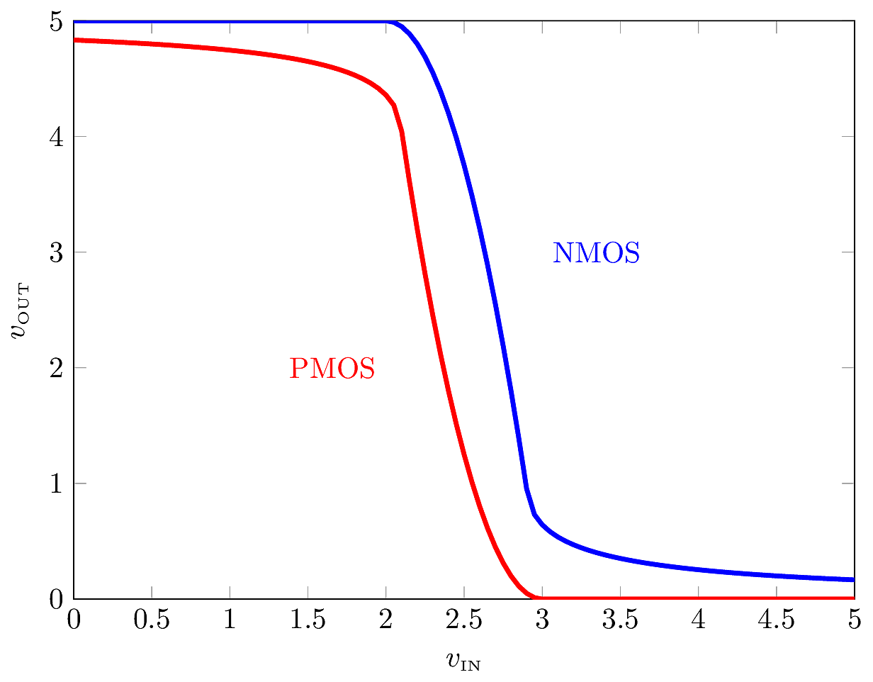
Our results show that both the NMOS and PMOS configurations have the same qualitative behavior. They both function as logic inverters. If we were to balance one of these circuits right in the center of its saturation region (II), where the slope is very steep, we could use it as an inverting amplifier. We will soon introduce linearized amplifier models that apply in the saturation region; it will be important to recognize that both NMOS and PMOS devices have the same linearized models in saturation, just as they show the same behavior in the RTL inverter configurations, even though they exhibit complementary logical behavior.
We may now go one level deeper and examine the MOSFET’s behavior in the saturation mode. First, let’s understand why it’s called “saturation.”’ Suppose we hold the gate potential fixed so that \(v_{\text{GS}}=1\,{\text{V}}\) and perform a DC sweep on \(v_{\text{DS}}\) while measuring the current.

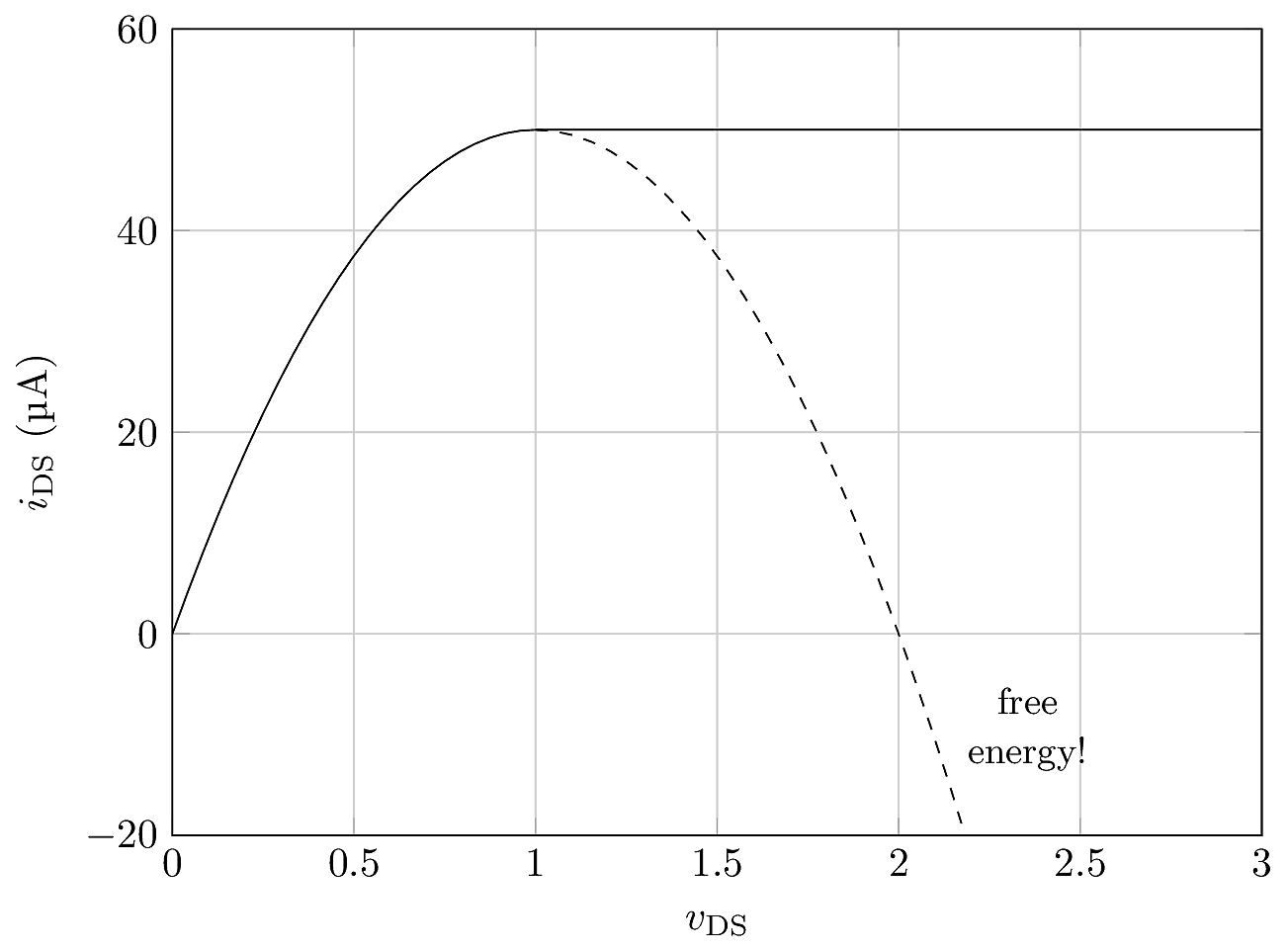
According to the triode equation, the current should be a parabola: \[i_\text{DS}= k\left((1)v_{\text{DS}}- \frac{1}{2}v_{\text{DS}}^2\right).\] But if that were true, the current would begin to decrease when \(v_{\text{DS}}>1\) (dashed curve below), and eventually the current would swing negative, creating an impossible free-energy device. Obviously this doesn’t happen, instead the device current rises monotonically until it reaches the peak of the parabola, and then flattens out at higher \(v_{\text{DS}}\) (solid curve). This is why it’s called saturation: when \(v_{\text{DS}}\) is swept from zero, \(i_\text{DS}\) increases until it saturates at a maximum value.
Since the saturation current is approximately constant, we may interpret the MOSFET as a nonlinear voltage controlled current source that depends on the gate voltage. For a first-order circuit analysis, we can replace the MOSFET symbol with a dependent current source. When a small signal is applied at the gate, we can write the gate voltage as a superposition of the DC signal (\(V_G\)) and the small signal (\(v_g\)). In that case we can linearize the current source by solving the first-order Taylor approximation:
\[i_D \approx V_{\text{GS}}+ \left(\left.\frac{d\,i_D}{d\,v_{\text{gs}}}\right|_{V_{\text{GS}}}\right) v_{\text{gs}}.\]
It will often be useful to analyze the small-signal equivalent circuit, which is obtained from the linearized model by zeroing out DC independent sources. For this purpose we may simplify the expression:
\[i_d \approx \left(\left.\frac{d\,i_D}{d\,v_{\text{GS}}}\right|_{V_{\text{GS}}}\right) v_{\text{gs}}.\]
Since the MOSFET takes a voltage as input and produces a current as output, it is conventionally interpreted as a transconductance amplifier. The amplifier’s transconductance gain, conventionally denoted as \(g_m\), is defined as the derivative of \(i_D\) with respect to \(v_{\text{GS}}\):
\[g_m \triangleq \left.\frac{d\,i_D}{d\,v_{\text{gs}}}\right|_{V_{\text{GS}}}\]
Then we can write the device’s small-signal behavior as simply
\[i_d = g_m\,v_{\text{gs}}.\]
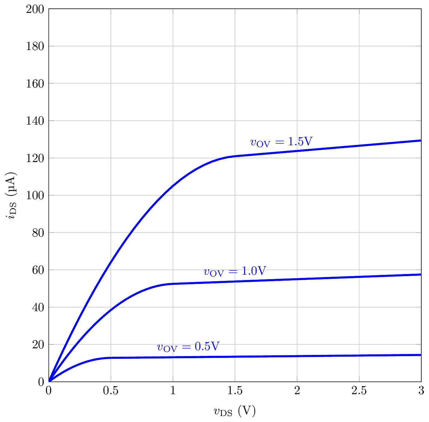
In a real MOSFET device, the saturation current is not perfectly constant with increasing \(v_{\text{DS}}\). Instead, we see an approximately linear increase with \(v_{\text{DS}}\), which can be partially explained as a variation in the MOSFET’s channel dimensions. From the circuit perspective, this behavior is modeled by augmenting the square-law equation with a “fudge factor” \(\lambda\):
\[i_\text{DS}= \frac{1}{2}kv_{\text{OV}}^2\left(1+\lambda\left|v_{\text{DS}}\right|\right).\]
Typically \(\lambda\) is in the range from \(0.01\,{\text{V}}^{-1}\) to \(0.1\,{\text{V}}^{-1}\). When including channel length modulation (CLM), the curves are not completely flat in saturation.
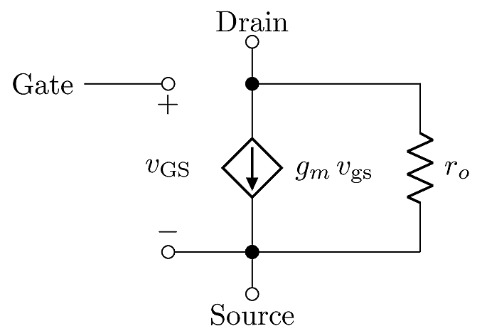
Since we consider the MOSFET to be a transconductance amplifier, we can interpret the slope due to CLM as the output resistance:
\[r_o \triangleq \left( \left.\frac{d\,i_D}{d\,v_{\text{DS}}}\right|_{\rm DC}\right)^{-1}.\]
In this definition, the derivative is evaluated at the DC operating point, which encompasses all the DC values of \(V_{\text{GS}}\), \(V_{\text{DS}}\) and \(I_D\).
The transconductance and output resistance can be calculated in a few different ways. We could measure these parameters experimentally by using an ammeter to observe the changes in \(i_D\) that result from small variations in \(v_{\text{GS}}\) and \(v_{\text{DS}}\). For hand analysis, we can directly integrate the device equations:
\[\begin{aligned} \frac{d\,i_D}{d\,v_{\text{GS}}} &= \left.\frac{d}{d\,v_{\text{GS}}} \left( \frac{1}{2}k\left(v_{\text{GS}}-{V_{\text{Th}}}\right)^2 \right)\right|_{\rm DC}\\ &= k\left(V_{\text{GS}}-{V_{\text{Th}}}\right)\\ &= kV_{\text{OV}}\end{aligned}\]
This tells us that the transconductance gain is directly proportional to the DC overdrive voltage.
Large Signal: \[\begin{aligned}
v_{\text{OV}}&= \left|v_{\text{GS}}\right| - \left|{V_{\text{Th}}}\right|\\
i_D &= \frac{1}{2}k\,v_{\text{OV}}^2 \\
\text{when~~} & \left|v_{\text{DS}}\right| > v_{\text{OV}}\\
\text{and~~} & v_{\text{OV}}>0.
\end{aligned}\] Small-Signal: \[\begin{aligned}
g_m &= k\,V_{\text{OV}}\\
&= \sqrt{2k\,I_D}\\
r_o &= \left(\lambda\,I_D\right)^{-1}\end{aligned}\]
In practice, it is often easier to select a DC bias current \(I_D\), rather than to directly control \(V_{\text{OV}}\). In that case, it is useful to express \(g_m\) in terms of \(I_D\):
\[\begin{aligned} kV_{\text{OV}}&= \sqrt{k\left(k\,V_{\text{OV}}^2\right)}\\ &= \sqrt{2k\,I_D}\end{aligned}\]
This expression tells us that the transconductance gain is proportional to the square root of the DC bias current.
Lastly, to calculate the output resistance we need to consider CLM:
\[\begin{aligned} r_o &= \left( \left.\frac{d}{d\,v_{\text{DS}}}\left(\frac{1}{2}kv_{\text{OV}}^2\left(1+\lambda\,v_{\text{DS}}\right)\right)\right|_{\rm DC}\right)^{-1}\\ &= \left( \frac{1}{2}kv_{\text{OV}}^2 \lambda\right)^{-1}\\ &= \frac{1}{\lambda\,I_D}\end{aligned}\]
This expression tells us that the output resistance is inversely proportional to the bias current. Since the transconductance increases with \(\sqrt{I_D}\), there is a tradeoff between transconductance and output resistance. This tradeoff will have important consequences for practical circuit design.
There are a few patterns that appear frequently in MOSFET circuits, and it will be useful to have their solutions available for reference. The two major cases are the diode connection and the passive resistor bias network. The third case is a combination of the first two. Additional configurations can be understood as special cases of these three configurations.
When the MOSFET’s gate is directly connected to the drain terminal, it is referred to as a “diode connection.” In this configuration, the drain terminal provides a negative feedback loop to the gate terminal, so that the circuit settles into a stable DC state. Since \(v_{\text{GS}}\) is determined by the voltage drop across \(R\), which is in turn determined by the current \(I_D\), the solution is governed by feedback:
\[\begin{aligned} V_{\text{GS}}= V_D &= V_{\text{DD}}- I_D R\\ I_D &= \frac{1}{2}k V_{\text{OV}}^2\\ &= \frac{1}{2}k \left( V_{\text{DD}}- I_D R - {V_{\text{Th}}}\right)^2\end{aligned}\]

The diode connection is guaranteed to always be in the saturation mode, since \(V_{\text{DS}}=V_{\text{GS}}\) it is always assured that \(V_{\text{DS}}>V_{\text{OV}}\).
To complete the solution, we define a variable \(x=\sqrt{I_D}\), and then arrange the above equation into a quadratic equation:
\[R\sqrt{\frac{k}{2}}x^2 + x - \sqrt{\frac{k}{2}}\left(V_{\text{DD}}-{V_{\text{Th}}}\right) = 0\]
Applying the quadratic formula:
\[\begin{aligned} x &= \frac{-1 \pm \sqrt{1+2kR\left(V_{\text{DD}}-{V_{\text{Th}}}\right)}}{R\sqrt{2k}}\\ \Rightarrow I_D = x^2 &= \frac{\left(-1 + \sqrt{1+2kR\left(V_{\text{DD}}-{V_{\text{Th}}}\right)}\right)^2}{2kR^2} \end{aligned}\]
In this very general case, resistors are placed adjacent to both the source and drain terminals, and the gate is biased at some constant voltage, such that the device is held in its saturation mode.

There are interactions at both the drain and source terminal:
\[\begin{aligned} V_D &= V_{\text{DD}}-I_D R_D\\ V_S &= I_D R_S\\ I_D &= \frac{1}{2}k\left( V_G - I_D R_S - {V_{\text{Th}}}\right)^2\end{aligned}\]
we solve this case in much the same way as the diode-connected circuit. By defining \(x=\sqrt{I_D}\), we can obtain a quadratic polynomial:
\[\begin{aligned} 0 &= R_S\sqrt{\frac{k}{2}}x^2 +x - \sqrt{\frac{k}{2}}\left(V_G-{V_{\text{Th}}}\right)\\ \Rightarrow x &= \frac{-1 \pm \sqrt{1 + 2kR_S\left(V_G-{V_{\text{Th}}}\right)}}{R_S\sqrt{2k}}\\ \textrm{and~} I_D &= x^2.\end{aligned}\]