
This summary covers some of the more important two-transistor configurations, which include MOSFET and BJT cascode and differential pair circuits, Darlington pairs, and some BiCMOS configurations (BiCMOS refers to combined MOSFET-BJT circuits).
The cascode is a “stack” of two transistors, and can be seen as a combination of common-source and common-gate circuits. The two circuits are folded together on a single branch, so that they share a single bias current source. This configuration is sometimes called a telescopic cascode.

Advantages:
High gain (product of CS and CG gains, approximately \((g_mr_o)^2\))
High output resistance (approximately \(g_mr_o^2\))
Disadvantages:
Limited output dynamic range
Very sensitive to bias errors
Low bandwidth
High noise
Cannot drive resistive loads
The folded cascode is the same concept as a cascode: a combination of CS and CG circuits. The difference is that the device type alternates between NMOS and PMOS, so we may combine NMOS CS with PMOS CG, or vice versa.

Advantages:
High gain (same as cascode)
Better dynamic range
Disadvantages:
Low bandwidth
High noise
Cannot drive resistive loads
The differential pair “steers” a bias current between two branches in response to an input differential signal. This is the front-end circuit for most op amps.

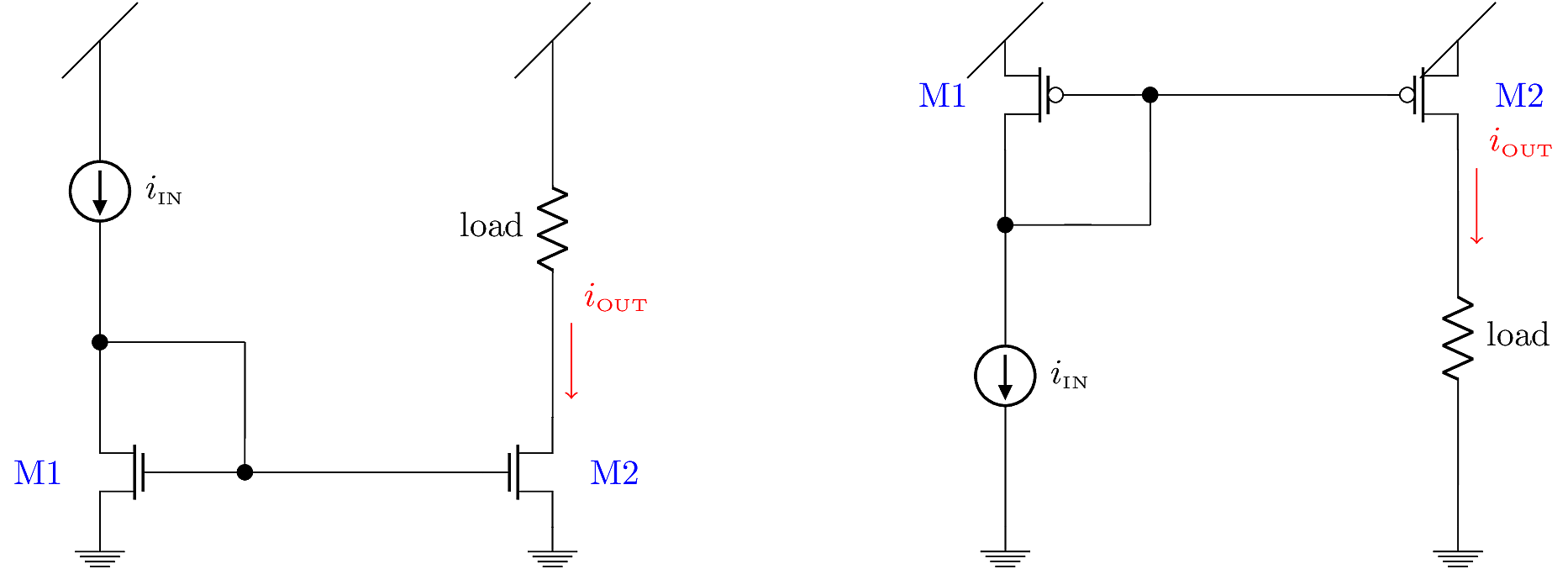
The current mirror duplicates a current. It is used as a bias current source for most of the other configurations.
The CMOS Push-Pull circuit is a non-linear Class B amplifier, which means there is no power dissipation when the signal is close to 0V. When \(v_\text{IN}> {V_{\text{ThN}}}\), the NMOS device turns on and behaves like a source follower. When \(v_\text{IN}< {V_{\text{ThP}}}\), the PMOS device turns on and behaves like a source follower. For loads with small resistance values, the push-pull amplifier is able to deliver a large amount of current, much more than a source follower. It is also more power efficient since it doesn’t use a DC bias current. The main drawback is distortion caused by the dead-zone when both devices are off.

To address excessive distortion in the Class-B push-pull amplifier, the input signal can be level-shifted to ensure that the NMOS and PMOS devices are never completely off. This is illustrated using ideal voltage sources in the figure below. In practice, there are numerous solutions to implement the level-shift. One of the simplest methods is to use two source followers to create signals \(v_\text{IN}+ {v_{\text{GS}}}_P\) and \(v_\text{IN}- {v_{\text{GS}}}_N\). The source followers’ \(v_{\text{GS}}\) values can be tuned to obtain a more linear transfer characteristic in the Class-AB circuit.

As with MOSFETs, we can place BJT devices in a “stacked” or telescopic cascode configuration. This corresponds to a cascade of Common-Emitter and Common-Base amplifiers. The small-signal behavior is a little bit different from the MOSFET case, since the CE stage is loaded by the \(r_{\pi}\) resistance in the CB stage.
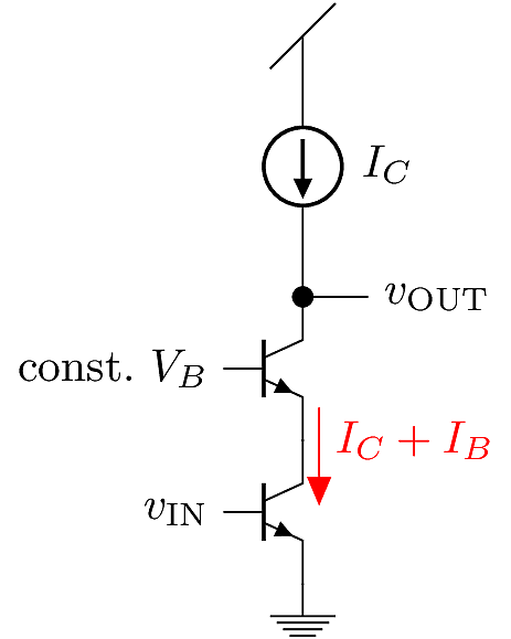
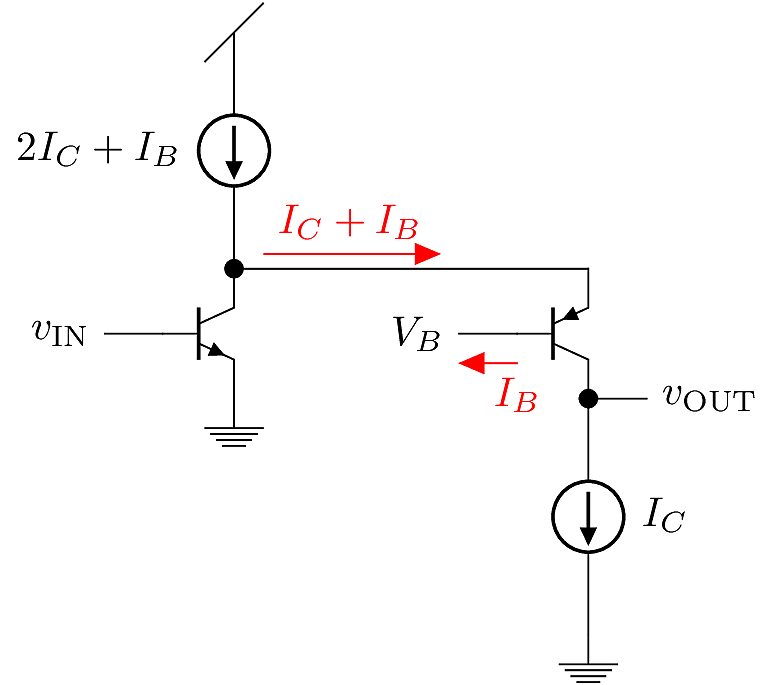
Since the BJT is essentially a current amplifier, we can also bias the CB stage with a constant base current instead of a constant base voltage:

BJT devices can also be configured in a folded cascode arrangement. The small-signal behavior is essentially the same as for the telescopic BJT cascode.
BJT differential pairs can be used to obtain higher gain than CMOS differential pairs. A major disadvantage is that they have a finite input resistance and require a DC input bias current on the base terminals.

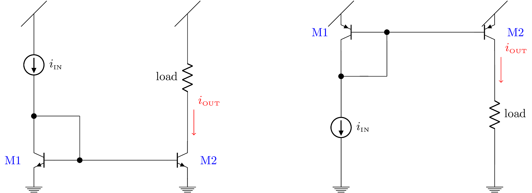
The BJT current mirror is similar to the MOS current mirror, except the BJT base current introduces a small systematic error (here “systematic” means a predictable, built-in error rather than a random error).
The Darlington Pair effectively multiplies the \(\beta\) value of a BJT device. Since the BJT is a current amplifier with \(I_E=\left(\beta+1\right)I_B\), we can cascade two stages by connecting the emitter from stage 1 into the base of stage 2. Then the total current gain is \(\left(\beta + 1\right)^2\). The Darlington Pair therefore behaves like a single BJT with an effective current gain of about \(\beta^2\). Since two base-emitter junctions now appear in series, the Darlington \(V_{BE}\) is about \(1.4\,\text{V}\) rather than \(0.7\,\text{V}\).

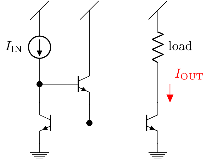
To reduce the systematic error in BJT current mirrors, an emitter follower can be introduced in the diode-connected feedback path as shown below. This has an effect similar to the Darlington Pair: the base current is multiplied twice, so the error current is made proportionally smaller. (This has three transistors, so it is not a two-transistor configuration, but it made sense to put it here).
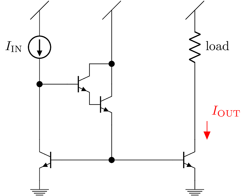
To obtain even better error compensation, a Darlington Pair can be used for the Emitter Follower:
The push-pull arrangement places an NPN “above” a PNP device as shown below. It is similar to two Emitter Followers folded together, but the behavior is more complicated than that. The devices are usually operated in a large-signal mode, where they alternately switch on and off. The switching activity creates non-linear distortion and noise, but if the switching occurs at a very high frequency, some of the distortion can be filtered out by the load. Push-pull configurations are popular for output stages and power amplifiers, since they can deliver large amounts of current and achieve very high dynamic range.

The push-pull amplifier shown above is called a Class B amplifier because there is a “dead zone” where both devices are off, so the current goes to zero. Up to now, we’ve only studied Class A circuits, which are defined by a constant bias current. The advantage of Class B circuits is that they don’t waste any power when the signal is idle. The disadvantage is the distortion created by the dead zone, which may require substantial post-amplifier filtering.
A compromise scheme is the Class AB push-pull design shown below. This is basically the same circuit as the Class B push-pull, except the dead zone is eliminated. The devices are never completely off. The idle current is not zero, but it can be quite small.

Class B and Class AB push-pull amplifiers can also be made with MOSFETs and Power MOSFET devices, but it is a little easier to study their BJT implementations.