
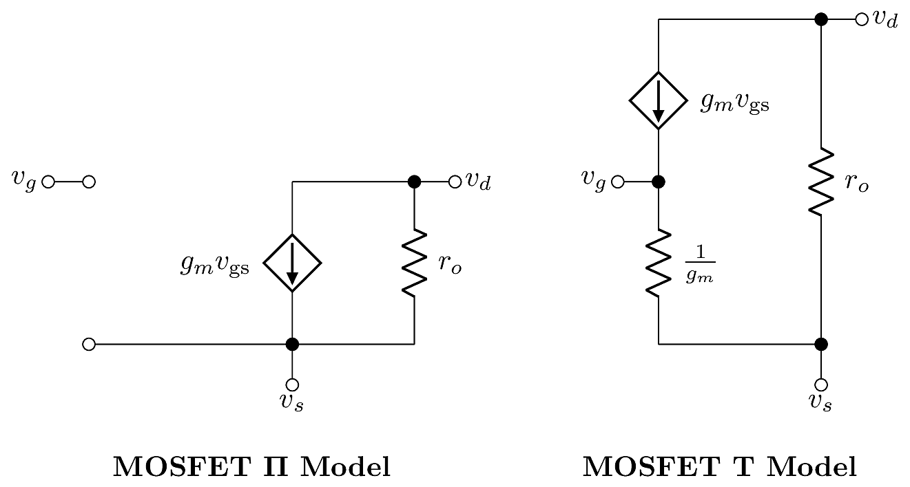
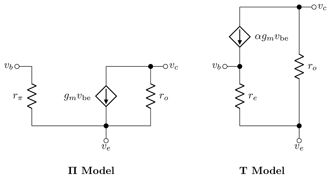
When a signal is sufficiently small, electronic devices can be approximated as linear networks. For transistor devices, there are two basic models:

These models are algebraically equivalent, which means that for a given set of terminal voltages \(v_g\), \(v_d\) and \(v_s\), the two models predict the exact same branch currents \(i_g\), \(i_d\) and \(i_s\). To satisfy this equivalency, there must be a relationship between \(r_\pi\) and \(r_e\), which can be solved by examining their currents in each model. In the \(\Pi\) model, the current into the gate is
\[i_g = \frac{v_{\text{gs}}}{r_\pi}.\]
In the T model, the current through \(r_e\) is a fictitious current equal to \(i_g+\alpha g_mv_{\text{gs}}\), so the gate current is expressed by
\[i_g = \frac{v_{\text{gs}}}{r_e}-\alpha g_mv_{\text{gs}}.\]
Equating these expressions gives
\[\frac{v_{\text{gs}}}{r_\pi} = \frac{v_{\text{gs}}}{r_e}-g_mv_{\text{gs}}.\]
Solving for \(r_e\), we find:
\[r_e = r_\pi \parallel \frac{1}{g_m}\]
For classical MOSFET and BJT devices, the model resistances are shown in the table below.
Parameter |
MOSFET |
BJT |
|---|---|---|
\(r_\pi\) |
\(\infty\) |
\(\frac{\beta}{g_m}\) |
\(r_e\) |
\(\frac{1}{g_m}\) |
\(\left(\frac{\beta}{\beta+1}\right)\left(\frac{1}{g_m}\right)=\frac{\alpha}{g_m}\) |
\(\alpha\) |
1 |
\(\frac{\beta}{\beta+1}\) |
In the MOSFET model, \(\alpha=1\) and \(r_\pi \rightarrow \infty\), so these aspects are simplified:
The small-signal parameters are obtained from the device equations, as summarized in the table below. These should already be familiar so are merely summarized here for review.
Parameter |
Symbol |
Units |
Definition |
Solutions |
|---|---|---|---|---|
Transconductance |
\(g_m\) |
A/V |
\(\frac{\delta i_d}{\delta v_{\text{gs}}}\) |
\(\sqrt{2KI_D}\), \(KV_{\text{OV}}\) |
Output resistance |
\(r_o\) |
\(\Omega\) |
\(\frac{\delta i_d}{\delta v_{\text{ds}}}\) |
\(\frac{1}{\lambda I_D}\) |
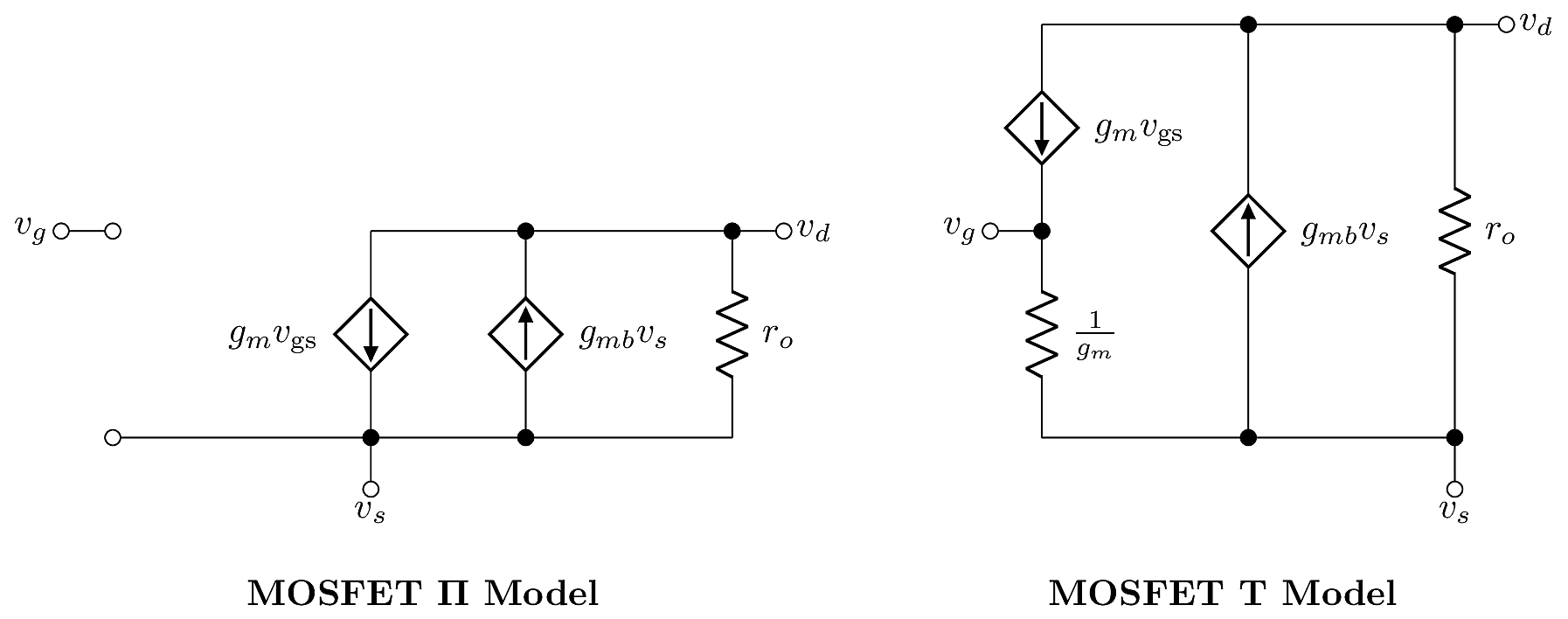
The basic MOSFET model can be improved upon by accounting for various second-order effects in the MOSFET’s behavior. One important example is the Body Effect, which accounts for signal-dependent variation in the MOSFET’s threshold voltage. When the source voltage \(v_S\) is not tied to the bulk voltage \(v_B\), the threshold voltage is altered:
\[{V_{\text{Th}}}= V_{T0} + \gamma\left(\sqrt{2\phi_b + v_{SB}} - \sqrt{2\phi_b}\right).\]
In the device’s saturation mode, the drain current is given by
\[i_D = \frac{1}{2}K\left(v_{\text{GS}}- {V_{\text{Th}}}\right)^2.\]
Clearly, the current depends separately on \(v_{\text{GS}}\) and \({V_{\text{Th}}}\), but \({V_{\text{Th}}}\) depends on \(v_S\). In the small-signal model, we can account for this effect by treating \(v_{\text{GS}}\) and \(v_S\) as independent variables. We define a body effect conductance:
\[g_{mb} \triangleq -\frac{\delta i_D}{\delta v_S} = KV_{\text{OV}}\frac{\delta {V_{\text{Th}}}}{\delta v_S} = g_m \frac{\delta {V_{\text{Th}}}}{\delta v_S},\]
where \(V_{T0}\) is the zero-bias threshold voltage (when \(v_S=v_B\)). For a particular source-bulk bias voltage \(V_{SB}\), it is convenient to represent the derivative as a constant parameter \(\eta\),
\[\eta \triangleq \frac{\delta {V_{\text{Th}}}}{\delta v_S} = \frac{\gamma}{2\sqrt{2\phi_b+V_{SB}}}.\]
Then the body effect conductance simplifies to
\[g_{mb} = \eta g_m\]
The respective contributions of \(g_m\) and \(g_{mb}\) are modeled by superposition in the small-signal equivalent circuit:
A small-signal configuration is defined by its signal flow from a designated input terminal to a designated output terminal. We are interested in the gain, defined by the ratio of output amplitude to the input amplitude, and also the equivalent terminal resistances, \(R_{\text{in}}\) and \(R_{\text{out}}\).
Input terminal: gate
Output terminal: drain
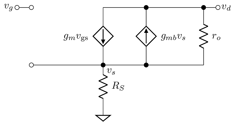
The small-signal common source configuration is represented by the model shown below (here we are using the \(\Pi\) model). The resistance \(R_S\) represents circuitry that could be present under the source terminal, depending on the specific circuit.
To find the gain, we need to solve the small-signal ratio:
\[A_{CS} = \frac{v_d}{v_g}.\]
In this model, the drain is a floating terminal, so there is no current into the drain. By Kirchoff’s Current Law, the sum of gate, drain and source currents must equal zero. Since the gate and drain currents are zero, the source current must also be zero. Therefore there is zero current through \(R_S\) and \(v_s=0\) for the purpose of this analysis, hence neutralizing the body effect. Then the drain voltage is \(v_d = -g_m r_o v_{\text{gs}}\), so the gain is
\(A_{CS} = -g_m r_o.\)
Since there is no current into the gate terminal of a MOSFET, the input resistance is infinite. The output resistance requires some analysis. To solve the equivalent resistance, we use the method shown in the model below.
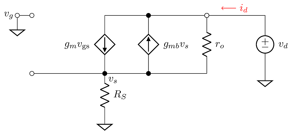
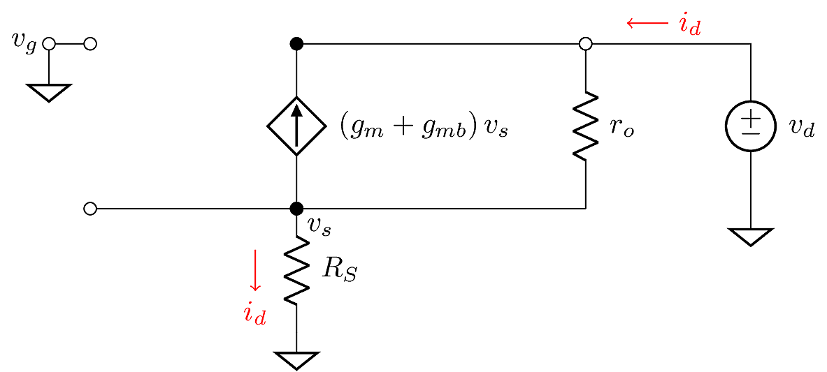
\[\begin{aligned} v_d &= v_s + \left(i_d + \left(g_m+g_{mb}\right)v_s\right)r_o\\ v_s &= i_d R_S\\ \Rightarrow v_d &= i_d R_S + i_d\left(1 + \left(g_m + g_{mb}\right)R_S\right)r_o\end{aligned}\]
Finally the output resistance is
\[R_{\text{out}}= \frac{v_d}{i_d} = R_S + r_o + \left(g_m + g_{mb}\right)r_oR_S\]
Input terminal: source
Output terminal: drain
The small-signal common source configuration is represented by the model shown below (here we are using the T model). The resistance \(R_D\) represents circuitry that could be present above the drain terminal.

Since the gate terminal is tied to a small-signal ground, \(v_{\text{gs}}= -v_s\). This allows a simplification to the small-signal circuit:

In the simplified model we can directly obtain the drain signal:
\[v_d = v_s + \left(g_m + g_{mb}\right)v_s r_o\]
Then the voltage gain is
\[A_{CG} = \frac{v_d}{v_s} = 1 + \left(g_m + g_{mb}\right)r_o.\]
Looking into the drain terminal, the output resistance is found by the exact same analysis used for the common-source configuration. The result is the same:
\[R_{\text{out}}= R_S + r_o + \left(g_m + g_{mb}\right)r_o R_S.\]
Looking into the source terminal, we find the configuration’s input resistance:
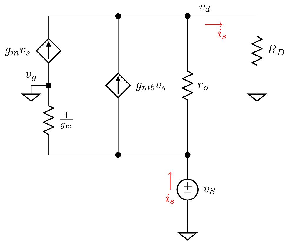
Here we apply Kirchoff’s Current Law:
\[i_s = \frac{v_d}{R_D}.\]
The current through \(r_o\) is the superposition of \(i_s\) with \(\left(g_m+g_{mb}\right)v_s\). Then the drain voltage is
\[v_d = i_sR_D = v_s + r_o\left(g_m+g_{mb}\right)-i_sr_o.\]
After grouping \(i_s\) and \(v_s\) terms, we arrive at the input resistance
\[R_{\text{in}}= \frac{v_s}{i_s} = \frac{R_D + r_o}{1+\left(g_m + g_{mb}\right)r_o}.\]
Input terminal: gate
Output terminal: source
The small-signal common drain configuration is represented by the model shown below (here we are using the T model).

The analysis is a little more intuitive with ground (\(v_d\)) placed on the bottom of the figure. After flipping the circuit over, we have this simplified model:

The current through \(r_o\) is a superposition of the \(g_m\) and \(g_{mb}\) contributions, so we have:
\[v_s = r_o\left(g_m\left(v_s-v_g\right) + g_{mb}v_s\right).\]
Now isolating the \(v_g\) and \(v_s\) terms, we can solve for the gain:
\[A_{SF}=\frac{v_s}{v_g} = \frac{g_m r_o}{1 + \left(g_m+g_{mb}\right)r_o}.\]
The gain is maximized when \(g_mr_o\gg 1\) (as large as possible). When considering the body effect, the maximum achievable gain is
\[A_{SF,\text{max}}=\frac{g_m}{g_m+g_{mb}} = \frac{1}{1+\eta}.\]
The input resistance into the gate is infinite. The output resistance seen looking into the source terminal is the same as the common-gate input resistance, with \(R_D=0\):
\[R_{\text{out}}= \frac{r_o}{1+\left(g_m+g_{mb}\right)r_o} \approx \frac{1}{g_m+g_{mb}}.\]
Input: base
Output: collector

Due to the finite value of \(r_\pi\), the base current is non-zero. By Kirchoff’s Current Law, the base current should equal the emitter current in this configuration, since the collector is left open. This means that \(r_\pi\) and \(R_E\) effectively form a single branch, constituting a voltage divider:
\[v_e = v_b\left(\frac{R_E}{R_E+r_\pi}\right).\]
Next, the current through \(r_o\) is \(g_mv_{\text{be}}\), so the collector voltage is
\[v_c = v_e - g_m r_o\left(v_b - v_e\right) = v_e\left(1+g_mr_o\right) - g_m r_o v_b.\]
Substituting for \(v_e\), we obtain the gain:
\[A_{CE} = \frac{v_c}{v_b} = \left(1+g_{m}r_o\right)\left(\frac{R_E}{R_E+r_\pi}\right)-g_{m}r_o= 1-g_{m}r_o\left(\frac{r_\pi}{R_E+r_\pi}\right).\]
In the BJT, \(r_\pi=\beta/g_m\), so if \(\beta\) is large, and \(g_{m}r_o\) is large, and \(R_E\) is small, then the gain simplifies to \(-g_{m}r_o\).
The input resistance is strongly affected by \(r_\pi\) and \(R_E\). In effect, the emitter resistance is amplified. This is most easily seen if, as an approximation, we temporarily omit \(r_o\) from the model. The resistance \(R_C\) is added so that there is a complete circuit around the collector and emitter terminals; it does not affect the analysis.

With this model, we can obtain two expressions for \(v_e\), one following the voltage drop across \(r_\pi\) and the other across \(R_E\):
\[v_e = R_E\left(g_mv_{\text{be}}+ v_{\text{be}}/r_\pi\right) = v_b - i_br_\pi.\]
We can simplify a bit by substituting \(r_\pi=\beta/g_m\):
\[g_mR_Ev_{\text{be}}\left(1+\frac{1}{\beta}\right) = v_b - i_b\frac{\beta}{g_m}.\]
If \(\beta \gg 1\) (which it usually is), then we can ignore the \(1/\beta\) term. Lastly we can substitute \(v_{\text{be}}=i_br_\pi\):
\[g_mR_E i_b \left(\frac{\beta}{g_m}\right) = v_b - i_b\left(\frac{\beta}{g_m}\right),\]
then arranging terms:
\[\begin{aligned} v_b &= i_b\left(\frac{\beta}{g_m}\right)\left(1+g_m R_E\right) \\ &\approx i_b \beta R_E\\ \Rightarrow R_{\text{in}}&\approx \beta R_E.\end{aligned}\]
To find the output resistance, we zero-out the base signal and apply a test voltage at the collector:
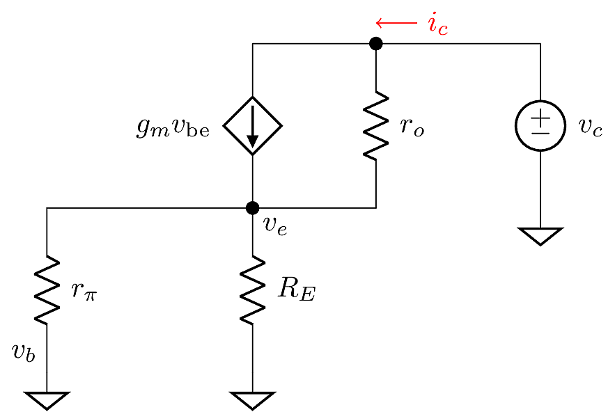
If \(r_\pi \gg R_E\), and noting that \(v_b=0\), we can make a slight simplification:
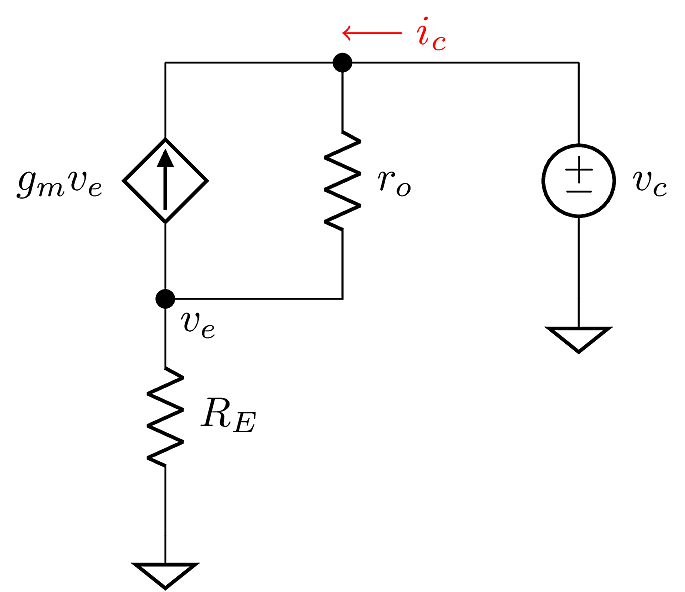
Then we can obtain two expressions for \(v_e\):
\[v_e = i_c R_E,\]
and
\[\begin{aligned} v_e &= v_c - r_o\left(g_mv_e + i_c\right)\\ \Rightarrow v_e\left(1+g_mr_o\right) &= v_c - i_cr_o\\ \Rightarrow v_e &= \frac{v_c - i_cr_o}{1+g_mr_o}\end{aligned}\]
Now set these equal to each other:
\[\begin{aligned} i_cR_E &= \frac{v_c - i_cr_o}{1+g_mr_o}\\ \Rightarrow v_c &= i_c\left(R_E+r_o+g_{m}r_oR_E\right)\end{aligned}\]
The result is identical to the MOSFET resistance at the drain terminal:
\[R_{\text{out}}= R_E+r_o+g_{m}r_oR_E.\]
Input: Emitter
Output: Collector
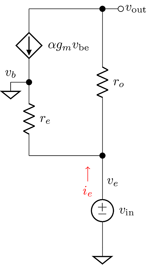
Since the Base terminal is connected to a constant bias voltage, it acts as a small-signal ground, hence \(v_{\text{be}}=-v_e\). This allows for a simplification:
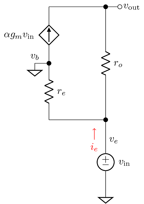
Following the voltage drop across \(r_o\) gives an expression for \(v_c\):
\[v_c = v_e + r_o\left(\alpha g_m v_e\right).\]
Isolating the terms for \(v_c\) and \(v_e\), we obtain the gain:
\[A_{CB} = \frac{v_c}{v_e} = 1+\alpha g_m r_o.\]
The emitter resistance is found by solving the emitter current, \(i_e\), that results from an applied test input \(v_e\). For this analysis, we allow that there may be some resistance \(R_B\), representing circuitry attached to the Base terminal. A similar resistor \(R_C\) is placed at the collector to model any load or bias circuitry that may be connected there. The resulting model is shown below.
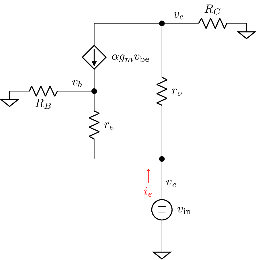
Analysis of the complete model, as shown above, is complicated. To simplify it, we divide the analysis into simplified cases.
This case is already represented by the simplified small-signal model we used for the gain analysis. In this case, \(r_e\) appears directly between the input terminal and small-signal ground. Since \(R_C\rightarrow \infty\), the output terminal is an open circuit, so we have \(i_b=i_e\) and therefore \(i_{\text{be}}=\alpha i_{\text{be}} - i_e\). Simplifying:
\[\begin{aligned} i_{\text{be}} &= \frac{i_e}{\alpha-1}\\ \Rightarrow v_e &= -i_{\text{be}} r_e = \frac{i_e r_e}{1-\alpha}\\ \Rightarrow R_{\text{in}}= \frac{v_e}{i_e} &= \frac{i_e r_e}{1-\alpha}\end{aligned}\]
Since \(\alpha \triangleq \beta/(\beta+1)\), we can further simplify as \(1/(1-\alpha)=\beta+1\). Then:
\[R_{\text{in}}= r_e\left(\beta+1\right) = \frac{\beta+1}{g_m}~~~~~ \text{ (case 1)}\]
In this case, once again we have an open circuit at \(v_{\text{out}}\) so \(i_b=i_e\). Since \(R_B>0\), we have \(v_b=i_e R_B\). As in case 1, we have \(i_{\text{be}}=\frac{i_e}{\alpha-1}\). The analysis differs from this step:
\[\begin{aligned} v_e &= v_b -i_{\text{be}} r_e = v_b - \frac{i_e r_e}{1-\alpha}\\ &= i_e R_B + \frac{i_e r_e}{1-\alpha}\\ \Rightarrow R_{\text{in}}&= R_B + r_e\left(\beta+1\right)~~~~~\text{(case 2)}\end{aligned}\]
So in effect, \(R_B\) makes a series contribution to the input resistance.
If both \(R_C\) and \(R_B\) are zero, then the \(\alpha i_{\text{be}}\) current source is shorted out. Then the input resistance is just
\[R_{\text{in}}= r_e \parallel r_o \approx \frac{1}{g_m}~~~~~\text{(case 3)}\]
where we note that \(r_o\) is typically much larger than \(1/g_m\), so its parallel contribution is negligible.
When \(R_C=0\), \(r_o\) is shunted to ground, so we can just analyze the \(r_e\) branch, and \(r_o\) will appear in parallel with that result. Since \(r_o\) is typically large, its parallel contribution can be ignored in this case. Then we have just one branch at \(v_e\), with \(i_e = -i_{\text{be}}\) and \(i_{\text{be}}=\alpha i_{\text{be}} - i_b\). Then we get
\[\begin{aligned} v_b &= i_b R_B\\ v_e &= v_b - i_{\text{be}}r_e\\ &= -i_{\text{be}}(1-\alpha)R_B - i_{\text{be}}r_e\\ \Rightarrow R_{\text{in}}&= \frac{R_B}{\beta+1} + r_e~~~~~\text{(case 4)}\end{aligned}\]
When \(R_C\) is “small”, the input resistance is essentially \(r_e=1/g_m\). When \(R_C\) is “large”, the input resistance is correspondingly large, approaching a maximum of \((\beta+1)/g_m + R_B\).
Input: base
Output: emitter
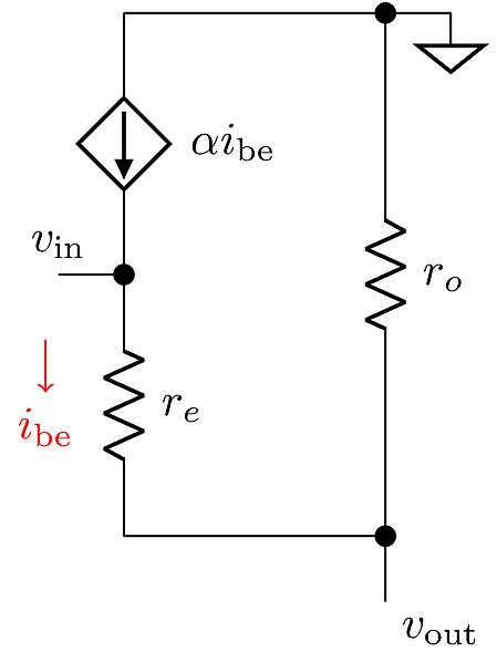
Since \(v_{\text{out}}\) is floating, the current through \(r_o\) is just \(i_{\text{be}}\), so \(v_{\text{out}}= i_{\text{be}}r_o\), therefore \(i_\text{be}=v_{\text{out}}/r_o\). At the same time, following the voltage drop across \(r_e\) gives \(v_{\text{out}}= v_{\text{in}}- i_{\text{be}}r_e\). Then we substitute for \(i_\text{be}\) and solve for \(v_{\text{out}}\):
\[\begin{aligned} v_{\text{out}}&= v_{\text{in}}- v_{\text{out}}\frac{r_e}{r_o}\\ \Rightarrow v_{\text{out}}&= v_{\text{in}}\left(\frac{1}{1+\frac{r_e}{r_o}}\right)\\ \Rightarrow \frac{v_{\text{out}}}{v_{\text{in}}} &= \frac{r_o}{r_o+r_e} &\approx 1 \text{V}/\text{V}\end{aligned}\]
The input resistance is the small-signal base resistance, the same as the Common-Emitter input resistance:
\[R_{\text{in}}= r_e + \left(\beta+1\right)R_E,\]
where \(R_E\) represents a resistance that may be connected at the emitter. In the open-circuit model, \(R_E\rightarrow \infty\) and so \(R_{\text{in}}\) is infinite.
The output resistance is the small-signal emitter resistance with \(R_C=0\), the same as Cases 3 and 4 in the Common-Base input resistance:
\[R_{\text{out}}= \frac{R_B}{\beta+1} + \frac{1}{g_m}.\]
In the open-circuit model where \(R_B=0\), the output resistance is just \(1/g_m\).