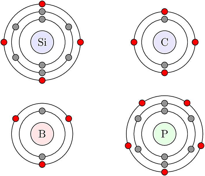
Most modern electronic devices are solid-state, meaning they are built from solid materials as opposed to gas, liquid or plasma (in contrast to vacuum tubes, for instance). Solid materials can be crystalline, where atoms are arranged with highly uniform geometry (e.g. diamond); or amorphous, where no uniform structure is discernible (e.g. glass); or they can be poly-crystalline, where small crystal grains are mashed together (e.g. granite).

The electronic properties of solids are determined by two key concepts: charge balance between an atom’s protons and electrons, and the octet rule which governs stability of electrons occupying an atom’s valence shell (i.e. the outermost orbit). In order for an atom to be electrically neutral, its total number of electrons must equal its total number of protons, which is equal to its atomic number.
The octet rule dictates that a stable electronic configuration should have precisely eight valence electrons. An atom can add to its valence shell in two ways: first, by participating in covalent bonds, which allow two electrons to be shared between neighboring atoms without upsetting their charge balance. Second, if the atom has fewer than eight valence electrons, it can capture a mobile electron from its environment. A captive electron upsets the charge balance, creating a surplus negative charge at the atom’s location, since there is no matching proton to balance it out.
In the converse scenario, if an atom has more than eight valence electrons, its surplus electron can escape and become mobile. The energy needed to separate a surplus electron is low enough that it can occur due to ambient thermal energy in the material. Once a surplus electron is separated from its atom, it becomes mobile and is available to conduct current.
The relationships among valence e- can be visualized using Lewis dot diagrams like the one shown below.

The processes of separating and binding electrons to atomic orbits is often described in terms of energy bands. At the atomic level, electrons have energy states determined by quantum physics. The energy states are quantized, like a collection of individual buckets that can each contain a single electron. In a sufficiently large volume of solid material, there can be a truly huge number of electrons and energy states which form an approximately continuous band of energy states.
All solids have two bands, called the valence and conduction bands, representing the allowed energy states of electrons within the material. In an insulator, there is a large gap between the valence and conduction bands, which means the electrons are tightly bound to their atomic orbits and require high energy to remove.

In a metal, the conduction band overlaps with the valence band so that electrons can easily change states and move around in the material.

A semiconductor has a smaller band gap than an insulator, allowing some electrons to transition into the conduction band, where they become mobile.
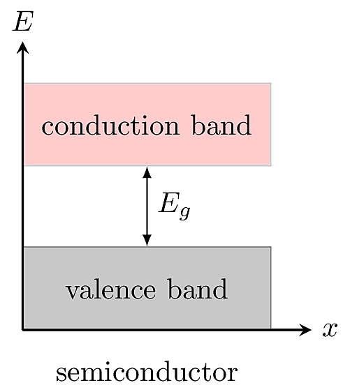
In a semiconductor, the valence and conduction bands are separated by a relatively small band gap \(E_g\). Thermal excitations can provide enough energy for a fraction of electrons to jump the gap. At ordinary temperatures, this results in a small number of electrons in the conduction band, so the material is slightly conductive. Electrons can also be promoted to the conduction band by absorbing a photon with energy greater than \(E_g\), so semiconductors are responsive to light and radiation.
energy levels are usually specified in electron Volts (eV), defined as voltage multiplied into the electronic charge \(q\). One eV is equivalent to 1.6e-19 J. The most common context is when a voltage \(V\) is applied across some material, thereby inducing a shift of \(qV\,\text{eV}\) in the energy levels within the material. So if \(V=1\,\text{{\text{V}}}\), we can say the energies are shifted by “one electron-volt” rather than 1.6e-19 Joules.
Band theory is a consequence of statistical mechanics; in a volume containing a very large number of atoms, the electrons’ energies are accounted for by a statistical distribution called the Fermi-Dirac distribution:
\[f(E) = \frac{1}{1+\exp\left(\frac{E-E_F}{k_B\,T}\right)}\]
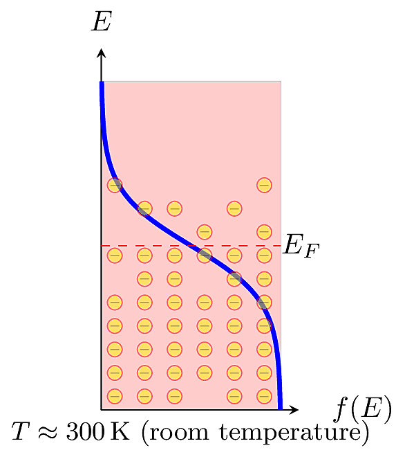
This equation is also called the Fermi function for short. For a given energy level \(E\), the Fermi function \(f(E)\) gives the probability of occupancy, meaning that an electron actually has that energy. In a specific material at thermal equilibrium, the distribution is centered around an energy called the Fermi Level, \(E_F\), defined as the energy level where the probability of occupancy falls to 0.5. The Fermi distribution depends on temperature. At absolute zero (\(T=0\)K), no electrons have energy above \(E_F\).
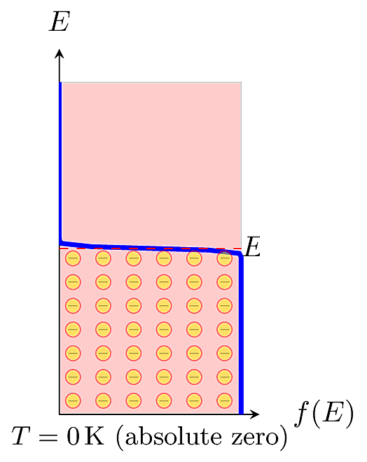
At higher temperatures, a fraction of electrons may be promoted to higher energy levels. In practice, we usually won’t need to know the precise value of \(E_F\). It is more important to know its relative distance from the valence or conduction band edges.
To understand the distribution of charges in a specific material, the Fermi function must be joined together with a function for the material’s Density of States. In a semiconductor or insulator, not every energy level is allowed. For example, there are no allowed states within the forbidden gap. Energy states within are “chopped out” from the distribution. Then the amount of mobile charge is determined by the distribution’s “tail,” the amount surviving in the conduction band.
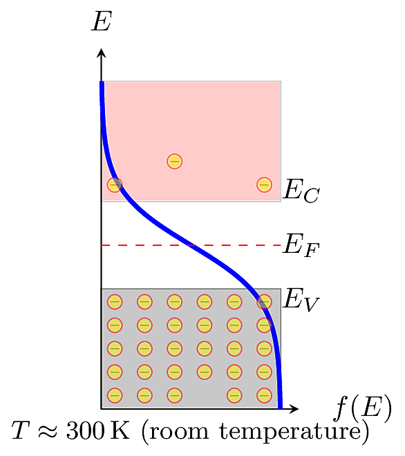
The Fermi function gives the probability that an energy state \(S\) at energy \(E\) is occupied by an electron. We could say the Fermi function has units of electrons per state. The density of states, \(N(E)\), is the fraction of allowed states that lie within a small “slice” between energies \(E\) and \(E+dE\), with units of states per energy level per volume. What we want to know now is: what is the density of electrons in the conduction band? The conduction-band electrons are free to conduct current in the material, and ultimately dictate the material’s behavior in a circuit.
\(N(E)\) reduces to a fairly simple quasi-constant value: nearly all electrons in the conduction band will “barely make it”, so they have energy barely greater than \(E_C\). Then \(N(E)\) can be approximated as an impulse function called the effective density of states, \(N_C\), which is known to be
\[N_C = 2 \left(2\pi\, m_e^*\,k_B\,T/h^2\right)^{3/2}\]
where \(m_e^*\) is the effective mass of an electron within the material, \(h\) is Planck’s constant, \(k_B\) is Boltzmann’s constant, and \(T\) is the temperature in Kelvin. For our purposes, one takeaway from this equation is that there is a non-simple dependence on temperature which will be obscured by layers of derivations.
When we multiply \(N(E)\) and \(f(E)\) together, the resulting units are
\[\frac{e^-}{\rm state} \times \frac{\rm states}{{\rm energy~level}\times{\rm volume}} = \frac{e^-}{{\rm energy~level}\times{\rm volume}},\]
where \(e^-\) is shorthand for “electrons.” To find the total density of mobile electrons in the material, we integrate \(f(E)\,N(E)\) over energies from \(E_C\) up to the vacuum energy \(E_0\) (If an electron has energy greater than \(E_0\), it will completely escape the material and fly off into space). The result reveals a great deal about the material’s electrical characteristics:
\[\begin{aligned} n &= \int_{E_C}^{E_0} f(E)\,N(E)\,dE\\ &\approx \int_{E_C}^{E_0} f(E)\,N_C\,\delta\left(E_C\right)\,dE\\ &= \frac{N_C}{1+\exp\left(\frac{E_C-E_F}{k_B\,T}\right)} \end{aligned}\]
If \(E_C-E_F > 4k_B\,T\), then we may further simplify the result:
\[n \approx N_C\exp\left(-\frac{E_C-E_F}{k_B\,T}\right).\]
When an \(e^-\) transitions into the conduction band, it leaves behind a hole (\(h^+\)) in the valence band. Holes are able to move around by being exchanged between neighboring valence shells in the material. A hole is considered to be a virtual particle capable of conducting current in parallel to the \(e^-\) current. Since mobile \(e^-\) and \(h^+\) are both available to carry current, they are referred to as mobile charge carriers. To determine the density of mobile \(h^+\) in a material, we again make use of the Fermi function. This time, we want to calculate the probability that a state is empty in the valence band, given by
\[1-f(E) = \frac{\exp\left(\frac{E-E_F}{k_B\,T}\right)}{1+\exp\left(\frac{E-E_F}{k_B\,T}\right)}.\]
Once again, we approximate the density of states as an impulse function at the valence band edge, where the effective density of states is \(N_V\). We repeat the integrate-and-approximate procedure from above to obtain
\[p \approx N_V\exp\left(-\frac{E_F-E_V}{k_B\,T}\right),\]
where \(N_V\) has the same form as the expression for \(N_C\):
\[N_V = 2 \left(2\pi\, m_h^*\,k_B\,T/h^2\right)^{3/2}\]
A semiconductor has a conduction band and a valence band, separated by a bandgap energy \(E_g\). The distribution of electron energies is parameterized by the Fermi level \(E_F\), which typically lies somewhere between the conduction and valence band edges, \(E_C\) and \(E_V\) (respectively). Electrons in the conduction band are able to conduct current. When an electron is promoted to the conduction band, it leaves a positive-charge hole in the valence band. Mobile holes conduct current in parallel to mobile electrons. The density of mobile electrons is
\[n \approx N_C\exp\left(-\frac{E_C-E_F}{k_B\,T}\right)\]
and the density of mobile holes is
\[p \approx N_V\exp\left(-\frac{E_F-E_V}{k_B\,T}\right).\]
In Si at room temperature, the effective density of states at the conduction band edge (\(N_C\)) and the valence band edge (\(N_V\)) are
\[\begin{aligned} N_C &= 2.86\,\times 10^{19}{\,\text{cm}^{-3}}\\ N_V &= 1.04\,\times 10^{19}{\,\text{cm}^{-3}}\end{aligned}\]
In Si, the bandgap is
\[E_g = 1.12\,\text{eV}\]
And an electron volt (eV) is the potential energy of one electron with a potential of 1:
\[1\,\text{eV}= 1.6\,\times 10^{-19}\,\text{J}\]