
While there are many design approaches for different types of MOSFET circuits, many common procedures for analog design can be characterized by the following steps:
Choose a circuit topology (e.g. CG, CS, cascode, etc).
Choose a bias current \(I_D\) (often based on specified constraints like gain, bandwidth, or power consumption).
Based on \(I_D\), compute the overdrive bias: \[V_{\text{OV}}= \sqrt{\frac{2I_D}{K}}.\]
Recall that \(K=\mu C_{\text{ox}}\left(\frac{W}{L}\right)\), and devices can have different \(W\) and \(L\), so you need to compute \(V_{\text{OV}}\) for each distinct geometry in the circuit.
From \(V_{\text{OV}}\), obtain the gate-source bias \(V_{\text{GS}}=V_{\text{OV}}+{V_{\text{Th}}}\) for each device.
Apply body effect correction if needed.
Apply Kirchoff’s Voltage Laws to solve the voltages at nets around the circuit.
Apply symmetry to solve remaining nets.
Apply the saturation condition, \(\left|V_{\text{DS}}\right| \geq V_{\text{OV}}\), to determine the max/min voltage range at the drain of each device. This usually gives the output dynamic range (or “swing”).
Now let’s explore these steps through a series of examples.
A “single-transistor” CS amplifier circuit is shown below. Device N1 is the amplifier, and the rest of the circuit is for biasing. The pair (N2,N3) forms a current mirror, as do the pairs (N2,N1) and (P2,P1). These mirrors setup a current steering bias so that all devices have the same DC bias current, \(I_D\). The value of \(I_D\) is configured by resistor \(R\).
At the gate of N1, we see a superposition of DC and AC signals:
\[v_{GN1}=V_{GN2}+v_{\text{in}}.\]
This means N1, N2 and N3 all have the same DC gate voltage, which also equals the drain voltage of N2. Similarly, P2 and P1 have the same gate voltage, which also equals the drain voltage of P2 and N3. So we have just three DC voltages to solve: \(V_{GN2},\) \(V_{GP}\), and \(V_{\text{OUT}}\). Let’s go through the steps:
The circuit topology is given.
\(I_D\) is chosen according to some given constraints and specifications.
Compute \({V_{\text{OV}}}_N=\sqrt{\frac{2I_D}{K_N}}\) and \({V_{\text{OV}}}_P=\sqrt{\frac{2I_D}{K_P}}\).
Compute \({V_{\text{GS}}}_N={V_{\text{OV}}}_N+{{V_{\text{Th}}}}_N\) and \(\left|{V_{\text{GS}}}P\right|={V_{\text{OV}}}_P+{{V_{\text{Th}}}}_P\). There is no body effect since all the source terminals are connected to their associated supply net.
Since all of the NMOS devices have their source voltages connected to ground, \(V_{GN2}={V_{\text{GS}}}_N\). For the PMOS devices, \(V_{GP}=V_{\text{DD}}-\left|{V_{\text{GS}}}_P\right|\).
The remaining net is \(V_{\text{OUT}}\). In this case, symmetry is not informative since we have a dual symmetry with (N1,N2) and (P1,P2), so the precise output offset voltage is ambiguous.
By the saturation condition, we need to satisfy \({V_{\text{DS}}}_{N1} \geq {V_{\text{OV}}}_N\). Since \({V_{\text{DS}}}_{N1}=V_{\text{OUT}}\), the minimum output voltage is \({V_{\text{OUT}}}_{\text{,min}}={V_{\text{OV}}}_N\). On the PMOS side, the condition is \(\left|{V_{\text{DS}}}_{P1}\right| \geq {V_{\text{OV}}}_P\). Since \(\left|{V_{\text{DS}}}_{P1}\right|=V_{\text{DD}}-V_{\text{OUT}}\), the maximum output is \({V_{\text{OUT}}}_{\text{,max}}=V_{\text{DD}}-{V_{\text{OV}}}_P\).
Now let’s put in some parameter values and work through the calculations. Suppose the bias current is given as \(I_D=250\mu\)A, and the supply voltage is \(V_{\text{DD}}=5\)V. The table below shows the default parameters for NMOS and PMOS devices in EveryCircuit:
| Parameter | NMOS | PMOS |
|---|---|---|
| \(K\) | 590\(\mu\)A/V\(^2\) | 453\(\mu\)A/V\(^2\) |
| \(\left|{V_{\text{Th}}}\right|\) | 0.43 V | 0.40 V |
| \(\lambda\) | 0.06 V\(^{-1}\) | 0.1 V\(^{-1}\) |
Next we crunch through the voltage calculations in the prescribed order:
| Potential | NMOS | PMOS |
|---|---|---|
| \(V_{\text{OV}}\) | 0.92057 V | 1.0506 V |
| V | 1.3506 V | 1.4506 V |
And the circuit’s node voltages are
| Net | Voltage |
|---|---|
| \(V_{GN2}\) | 1.3506 V |
| \(V_{GP}\) | 3.5494 V |
| \(V_{\text{OUT}}\) | underdetermined |
Then the output swing:
| \(v_\text{OUT}\) min | \(v_\text{OUT}\) max | Output Swing |
|---|---|---|
| 0.92057 V | 3.9494 V | 3.0288 V |
After all these calculations, the last thing we do is calculate the bias resistor \(R\):
\[R = \frac{V_{\text{DD}}-V_{GN2}}{I_D} = 14.6\,\text{k}\Omega.\]
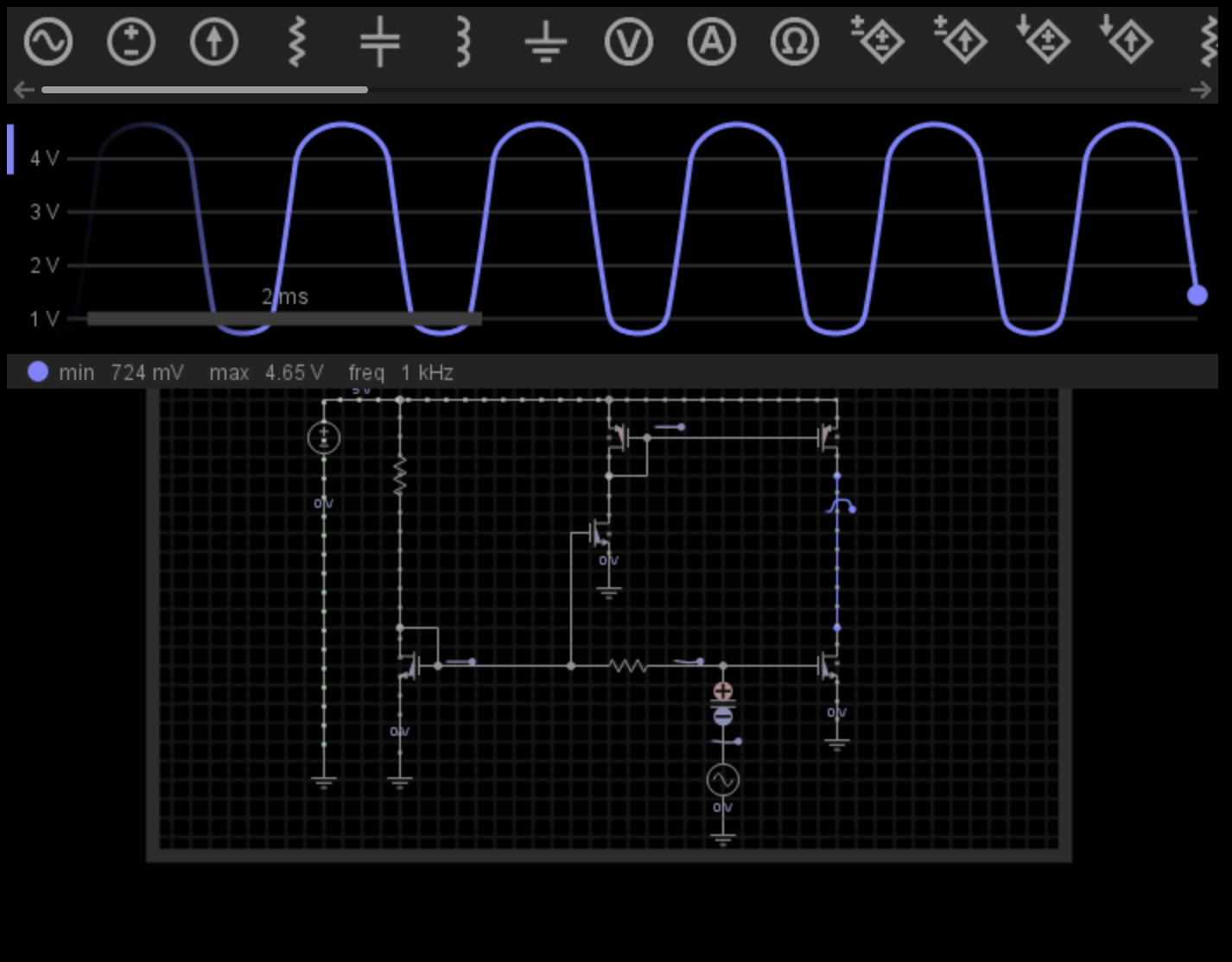
After implementing the design in EveryCircuit, the net voltages are confirmed to within a small percentage of error. The output swing is trickier, since the output signal can physically swing beyond the maximum and minimum limits. The signal is not clipped, it is distorted, as seen in the screenshot below.
Next we analyze a five-transistor Operational Transconductance Amplifier (OTA) circuit with bias network. The standard circuit for this configuration is shown below. Devices (N1,N2) form a differential pair, and current mirrors are formed by (N3,N4) and (P1,P2). Since the bias current is split in half by the differential pair, the bias current in N3 and N4 is double that of the other devices.
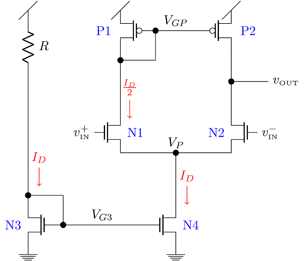
This circuit receives a differential input signal, \(v_\text{IN}={v_\text{IN}}^+ - {v_\text{IN}}^-\), and produces a single-ended output signal. OTA circuits are frequently used as the first stage of an op amp. Since op amps are typically used in negative feedback configurations, we will assume that this OTA is placed within a negative-feedback system. In that case, the virtual short effect should force \(v_\text{IN}^+ \approx v_\text{IN}^-\), i.e. the two input signals will be close to the same value (though not exactly the same). When the two inputs are equal, the OTA is said to be in its common-mode configuration. For our analysis here, we will set \(v_\text{IN}^+=v_\text{IN}^-=v_\text{ICM}\), where \(v_\text{ICM}\) is called the common-mode input signal.
Given a particular bias current \(I_D\) and common-mode input \(v_\text{ICM}\), we should be able to solve for the remaining nets, \(V_{G3}\), \(V_P\), \(V_{GP}\) and \(V_{\text{OUT}}\). Let’s go through the analysis steps.
The topology here is given as an OTA.
A bias current \(I_D\) is chosen somehow, and is taken as a given parameter.
Now the \(V_{\text{OV}}\) value for N3 and N4 is
\[{V_{\text{OV}}}_3 = \sqrt{\frac{2I_D}{K_{N3}}}.\]
For N1 and N2, the bias current is cut in half. Also, the differential pair devices typically have a distinct geometry from the bias devices, so
\[{V_{\text{OV}}}_1 = \sqrt{\frac{I_D}{K_{N1}}}.\]
Lastly, the PMOS devices have
\[{V_{\text{OV}}}_P = \sqrt{\frac{I_D}{K_P}}.\]
Next, the \(V_{\text{GS}}\) value for each device is found as \(\left|V_{\text{GS}}\right| = V_{\text{OV}}+\left|{V_{\text{Th}}}\right|\). There can be a body effect on N1 and N2, but we will ignore it for now since it depends on \(v_\text{ICM}\).
Now the net voltages are found:
\(V_{G3} = {V_{\text{GS}}}_{N3}\)
\(V_P = v_\text{ICM}- {V_{\text{GS}}}_{N1}\)
\(V_{GP}=V_{\text{DD}}-\left| {V_{\text{GS}}}_{P}\right|\)
In this circuit, the output offset \(V_{\text{OUT}}\) can be determined by symmetry between P1 and P2. Since these devices have the same gate and source voltages, and also the same current, the output should stabilize to \(V_{\text{OUT}}\approx V_{GP}\).
In the OTA, saturation conditions constrain both the input and the output:
Input Common-Mode Range (ICMR) — First, on the low side of \(v_\text{ICM}\), in order to keep N4 in saturation, we require \(V_P>{V_{\text{OV}}}_{N4}\). Since \(V_P\) depends on \(v_\text{ICM}\), we have a constraint on the input:
\[v_\text{ICM}> {V_{\text{OV}}}_{N4}+{V_{\text{GS}}}_{N1}.\]
Next, on the high side of \(v_\text{ICM}\), we need to keep N1 and P1 in saturation. This means we need \(V_{\text{OUT}}-V_P > {V_{\text{OV}}}_{N1}\), and \(V_{\text{DD}}-V_{\text{OUT}}> {V_{\text{OV}}}_P\). Hypothetically, if we squeeze N1 to the limit, then
\[V_{\text{OUT}}\rightarrow V_P + {V_{\text{OV}}}_{N1} = v_\text{ICM}- {{V_{\text{Th}}}}_N\]
Then, looking at the condition for P1, and using the above hypothesis for \(V_{\text{OUT}}\), we get:
\[V_{\text{DD}}- v_\text{ICM}+ {{V_{\text{Th}}}}_N > {V_{\text{OV}}}_P\]
Now rearrange to find the limit on \(v_\text{ICM}\):
\[v_\text{ICM}< V_{\text{DD}}- {V_{\text{OV}}}_P + {{V_{\text{Th}}}}_N.\]
This result shows that if \({V_{\text{OV}}}_P < {{V_{\text{Th}}}}_N\), then the upper limit is just \(V_{\text{DD}}\), so \(v_\text{ICM}\) can swing all the way to the positive rail.
Output Swing — On the output side, we already found the limits while analyzing the ICMR. These were:
\[\begin{aligned} v_\text{OUT}&< V_{\text{DD}}- {V_{\text{OV}}}_P\\ v_\text{OUT}&> V_P + {V_{\text{OV}}}_{N1} = v_\text{ICM}- {{V_{\text{Th}}}}_N \end{aligned}\]
The output swing is constrained by \(v_\text{ICM}\) on the low side. On the high side, we note that \(V_{\text{OUT}}=V_{GP}=V_{\text{DD}}- {V_{\text{OV}}}_P- {{V_{\text{Th}}}}_P\). This means that, relative to its DC bias point, the highest \(v_\text{OUT}\) can swing is \(V_{\text{OUT}}+ {{V_{\text{Th}}}}_P\). On the low side, the limit depends on \(v_\text{ICM}\), so the low-side swing can be made larger than the high-side swing by choosing a suitable \(v_\text{ICM}\). If the signal is a sinusoid, the amplitude is limited by the high-side, so the maximum zero-to-peak output amplitude is \({{V_{\text{Th}}}}_P\).
At last we can supply some numbers and complete an example design. Using the device parameters given in the previous example, and keeping the same bias current of \(250\,\mu\)A, and supply voltage \(V_{\text{DD}}=5\,\text{V}\), we can fill in the table of results below.
| Variable | Value |
|---|---|
| \({V_{\text{OV}}}_{N3}\) | 0.92057 V |
| \({V_{\text{OV}}}_{N1}\) | 0.65094 V |
| \({V_{\text{OV}}}_{P}\) | 0.74288 V |
| \(V_{G3}\) | 1.3506 V |
| \(V_P\) | \(v_\text{ICM}-1.0809\) V |
| \(V_{GP}\) | 3.8571 V |
| \(V_{\text{OUT}}\) | 3.8571 V |
| \(v_\text{ICM}\) (min) | 2.0015 V |
| \(v_\text{OUT}\) (max) | 4.2571 V |
| \(v_{\text{out}}\) (max amplitude) | 0.4 V |
Based on the numbers above, we can choose a safe \(v_\text{ICM}\) of 2.5V, which is conveniently equal to \(V_{\text{DD}}/2\). That should define \(V_P\) at 1.4191V. We can also use the same value for \(R\) that we obtained in the common-source example, about 15k\(\Omega\). After simulating this design in EveryCircuit, these bias results are verified to an accuracy within 2%. A transient simulation, shown below, confirms that output distortion begins on the high side, as expected.
