
The Field Effect Transistor (FET) was first described by Julius Edgar Lilienfeld in a 1926 patent. The basic concept is very similar to modern FET devices, but the devices could not be manufactured in Lilienfeld’s day since they require precise composition and structure at microscopic dimensions. The first modern Metal Oxide Semiconductor (MOS) FET device was demonstrated at Bell Labs in 1960 by Atalla and Kahng.
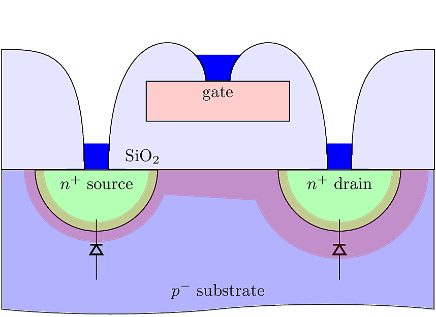
The figures below show an overhead layout and a cross sectional illustation of a standard N-type MOSFET. This device is fabricated on a P-type substrate with weak doping, indicated as \(p^-\). The Source and Drain regions are implanted with strong N-type doping, indicated as \(n^+\). A layer of insulation, usually silicon dioxide (SiO\(_2\), also called the “glass” layer), is grown or deposited on the surface. The region between the Source and Drain terminals is called the channel with length \(L\). Suspended above the channel is the Gate terminal, which is a deposited layer of poly-crystaline Si (“polysilicon” or just “poly” for short).

The basic structure of the 1960 MOSFET is still used up to the present day. Variations on this structure have been at the cutting edge until very recently. Today we see competition from alternative nano-wire and finFET structures which will be discussed later; first we’ll study the classic bulk MOSFET device that is used in nearly all integrated circuits produced since the 1980s.
The standard MOSFET device, shown in the cross-sectional illustration above, consists of a silicon wafer (called the substrate or bulk). In many cases the wafer is doped P-type with a relatively weak dopant concentration (weak doping is indicated as \(p^-\)). On the surface of the wafer is a layer of insulating SiO\({}_2\) called the oxide. A short distance above the wafer surface, the oxide is thinned to deposit a layer of poly-silicon which forms the device’s gate terminal. The oxide thickness below the gate establishes an incremental gate capacitance:
\[C_{\text{ox}}^\prime = \frac{\epsilon_{\rm ox}}{t_{\rm ox}},\]
with units of Farad per \(\mu\)m\(^2\). The total capacitance depends on the area under the gate, equal to \(W\times L\). One of the main benefits of a capacitive gate is that it prevents any DC current from flowing into the device’s gate terminal. This makes the MOSFET nearly ideal for use as a low-frequency voltage amplifier, and is a crucial property for energy efficient large-scale logic circuits.
For some very small devices, with channel lengths below 90nm, \(t_\text{ox}\) is small enough to permit quantum tunneling through the oxide. This phenomenon, called gate leakage, is one of many problems that has led the industry to modify the classic MOSFET structure. More recent structures, like the FinFET, are increasingly favored in new technologies. We will examine the FinFET structure in a later chapter.
In an industrial setting, manufacturers and process physicists determine many of the device’s properties, like the doping concentrations, oxide thickness below the gate, minimum dimensions and spacings of objects, depth of the source and drain implants, and so on. But chip-level designers have the freedom to manipulate two important dimensions: the device’s length \(L\), defined as the spacing between the source and drain terminals, and the width \(W\). These dimensions are determined by the device’s design layout. A layout designer has considerable freedom to manipulate the device geometry so long as the basic process design rules are obeyed.
To understand the operation of the MOSFET device, we begin with the case of zero gate bias. This means that the gate and substrate are at the exact same potential. Since the device is physically symmetrical, there is no special distinction between the source and drain terminals other than that the drain is assumed to be at a higher potential than the source. We will assume that \(V_S \geq 0\) and \(V_D \geq V_S\). The source and drain regions form PN junctions with the substrate. Since the substrate is weakly doped, the junctions are one-sided, and a depletion region extends around the terminals into the bulk. Generally the depletion is thicker around the drain, and can extend all the way across the surface connecting between the source and drain. In this condition, the device acts like a capacitor.
To a first approximation, no current flows between the source and drain when the gate voltage is zero. More accurately, a small leakage current flows due to generation/recombination and other effects in and around the depletion region.
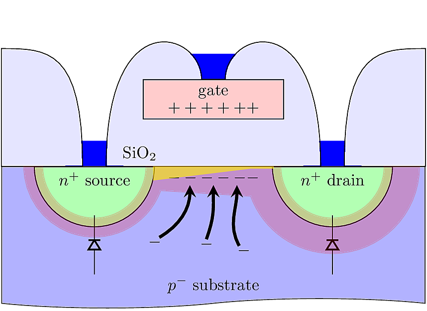
When \(V_G\) is slightly greater than zero, but less than the device’s threshold voltage, majority carriers (holes) are repelled from the region beneath the gate. Minority carriers (electrons) are attracted from the bulk. The minority carriers aggregate at the Si surface, just beneath the oxide layer, resulting in an inversion of mobile charge polarity in the MOSFET channel between the source and drain.

In this mode, the potential along the channel is nearly constant, and the voltage drop between \(V_D\) and \(V_S\) occurs close to their junctions. Hence there is no net \(\mathcal{E}\)-field in the channel, and no drift current flows. The excess minority charges tend to diffuse into the Source and Drain junctions, in a process similar to a weakly forward biased diode. Since the weak inversion current flows primarily by diffusion across junctions, the device has an exponential current similar to a diode. The Source and Drain diffusion currents are
\[\begin{aligned} I_{\rm source} &= I_0 \exp\left(\frac{\phi-V_S}{U_T}\right)\\ I_{\rm drain} &= I_0 \exp\left(\frac{\phi-V_D}{U_T}\right)\end{aligned}\]
where \(I_0\) is a scale current and \(\phi\) is the channel potential. The channel potential is determined by a capacitive divider which forms between the oxide capacitance and the depletion capacitance under the channel. Let \(\kappa \triangleq C_{\rm dep}/\left(C_{\rm ox}+C_{\rm dep}\right)\) be the divider ratio, then the channel potential is
\[\phi=\kappa V_G.\]
Most often \(\kappa\approx 0.7\), but it can vary considerably since \(C_{\rm dep}\) is a function of the channel charge. The total current is the difference between the Drain and Source currents:
\[\begin{aligned} I &= I_0\left[\left(\frac{\kappa V_G-V_S}{U_T}\right) - \left(\frac{\kappa V_G-V_D}{U_T}\right)\right]\\ &= I_0\exp\left(\frac{\kappa V_G - V_S}{U_T}\right)\left[1-\exp\left(\frac{-V_{DS}}{U_T}\right)\right]\end{aligned}\]
For a bulk MOSFET device, the scale current \(I_0\) can be shown to be
\[I_0 = \left(\frac{2\mu_nC_{\rm ox}^\prime U_T^2}{\kappa}\right) \left(\frac{W}{L}\right)\exp\left(\frac{-\kappa V_{\rm Th}}{U_T}\right).\]
When \(V_{DS}\) is greater than about 100mV, the current becomes insensitive to \(V_{DS}\) and the device is said to be in substhreshold saturation. In this mode we can use the approximate expression,
\[I_D \approx I_0 \exp\left(\frac{\kappa V_G - V_S}{U_T}\right).\]
As the gate voltage is increased, a larger amount of charge is accumulated in the channel, eventually supporting a voltage drop along the channel. This means an \(\mathcal{E}\)-field begins to appear resulting in a drift current between the drain and source. This transition occurs when \(V_G \approx {V_{\text{Th}}}\), and the channel is said to be strongly inverted.

In this mode, the potential along the channel changes gradually from \(V_S\) to \(V_D\). Let \(\phi_s\left(x\right)\) be the surface potential at some point \(x\) along the channel, so that \(\phi(0)=V_S\) and \(\phi(L)=V_D\). Now consider a small “slice” of width \(dx\), the total capacitance of the oxide under the gate is
\[C_{\textrm{\tiny slice}}= C_{\text{ox}}^\prime W dx.\]
(Recall that \(C_{\text{ox}}^\prime\) is capacitance per area, so we have to multiply the total slice area \(W dx\) to get the total capacitance.)

The charge stored in a capacitor is \(Q = CV_C\), where \(V_C\) is the potential across the capacitor. In the case of a MOSFET, the gate potential needs to exceed \({V_{\text{Th}}}\) before an appreciable charge is stored. Therefore we have to subtract \({V_{\text{Th}}}\) from the potential across \(C_{\textrm{\tiny slice}}\):
\[Q_{\textrm{\tiny slice}}\left( x \right) = C_{\text{ox}}W dx \left(V_G - \phi_s\left(x\right) - {V_{\text{Th}}}\right)\]
The total current in the channel is constant, and is generated by the \(\mathcal{E}\)-field oriented from the drain toward the source:
\[\begin{aligned} I_D &= \mu_n Q_{\textrm{\tiny slice}}\mathcal{E}\left(x\right), \\ \mathcal{E}\left(x\right)&= -\frac{d\phi_s\left(x\right)}{dx}\end{aligned}\]
Combining these expressions, we can apply a differential trick:
\[I_Ddx = -\mu_n Q_{\textrm{\tiny slice}}d\phi_s,\]
and then we can simultaneously integrate the left side over the length of the channel from \(x=0\) up to \(x=L\), and on the right side over the potential from \(\phi_s(0)=V_S\) up to \(\phi_s(L)=V_D\):
\[\begin{aligned} \int_0^L I_D dx &= \int_{V_S}^{V_D} \mu_n C_{\text{ox}}^\prime W \left(V_G - \phi_s\left(x\right)- {V_{\text{Th}}}\right) d\phi_s \\ \Rightarrow I_D L &= \left[ \frac{1}{2}\mu_n C_{\text{ox}}^\prime W \left(V_G - \phi_s - {V_{\text{Th}}}\right)^2 \right]_{V_S}^{V_D} \\ \Rightarrow I_D &= \frac{1}{2}\mu_n C_{\text{ox}}^\prime \frac{W}{L} \left[ \left(V_{GS} - {V_{\text{Th}}}\right)^2 - \left(V_{GD} - {V_{\text{Th}}}\right)^2 \right] \end{aligned}\]
This result describes the triode mode of operation. It can be rearranged algebraically into the more familiar form:
\[\begin{aligned} I_D &= \frac{1}{2}\mu_n C_{\text{ox}}^\prime \frac{W}{L} \left[ \textcolor{red}{V_{GS}^2 - V_{GD}^2} -2V_{GS}{V_{\text{Th}}}+ \cancel{{V_{\text{Th}}}^2} + 2V_{GD}{V_{\text{Th}}}- \cancel{{V_{\text{Th}}}^2} \right]\\ &= \frac{1}{2}\mu_n C_{\text{ox}}^\prime \frac{W}{L} \left[ 2V_G V_{DS} - \left(V_D^2 - V_S^2\right) + \textcolor{red}{2{V_{\text{Th}}}\left(V_{GD}-V_{GS}\right)}\right]\\ &=\frac{1}{2}\mu_n C_{\text{ox}}^\prime \frac{W}{L} \left[2V_G V_{DS} \textcolor{red}{-2V_S V_{DS}} - 2{V_{\text{Th}}}V_{DS} - \left(V_D^2 - V_S^2\right) \textcolor{red}{+2V_S V_{DS}} \right]\\ &= \frac{1}{2}\mu_n C_{\text{ox}}^\prime \frac{W}{L} \left[ 2\left(V_{GS}-{V_{\text{Th}}}\right)V_{DS} - \left(V_D^2 - 2V_D V_S + V_S^2\right) \right]\\ &= \mu_n C_{\text{ox}}^\prime \frac{W}{L} \left[\left(V_{GS}-{V_{\text{Th}}}\right)V_{DS} - \frac{1}{2}V_{DS}^2 \right] \end{aligned}\]
When the MOSFET is in strong inversion, with \(v_{\text{GS}}> {V_{\text{Th}}}\), the current depends strongly on \(v_{\text{DS}}\). When \(v_{\text{DS}}\) is increased from zero, the device current also increases until it reaches a maximum value. The value of the maximum is obtained by taking the derivative of \(i_D\) with respect to \(v_{\text{DS}}\).
The derivative should cross zero at the maximum point:
\[\begin{aligned} \frac{di_D}{dv_{\text{DS}}} &= \mu_nC_{\text{ox}}^\prime\frac{W}{L}\left[\left(V_{GS}-{V_{\text{Th}}}\right) - V_{DS} \right] = 0\\ \Rightarrow v_{\text{DS}}&= v_{\text{GS}}- {V_{\text{Th}}}\textrm{~when~} i_D \textrm{~is~maximum.}\end{aligned}\]
The device current at this maximum point is
\[i_D^\star = \frac{1}{2}\mu C_{\text{ox}}^\prime\frac{W}{L} \left(v_{\text{GS}}- {V_{\text{Th}}}\right)^2,\]
note we have used the star (\(\star\)) superscript to indicate that this is a somewhat idealized result.
Once \(v_{\text{DS}}\) exceeds \(v_{\text{GS}}-{V_{\text{Th}}}\), the current is no longer strongly dependent on \(v_{\text{DS}}\), so it is said to be saturated. To put it another way, we consider the channel to be fully formed when \(v_G - \psi_s \geq {V_{\text{Th}}}\), but if \(v_D\) is large this will cease to be true in the vicinity of the drain terminal. When \(v_{GD} < {V_{\text{Th}}}\), the channel is not fully inverted all the way from the drain to the source, and is said to be “pinched off” in that it fizzles out part way across. Then by a simple analysis we can obtain the condition for saturation:
\[\begin{aligned} v_{GD} < {V_{\text{Th}}}\\ \Rightarrow -v_{GD} > -{V_{\text{Th}}}\\ \Rightarrow v_D > v_G - {V_{\text{Th}}}\\ \Rightarrow v_D - v_S > v_G - v_S - {V_{\text{Th}}}\\ \Rightarrow v_{\text{DS}}> v_{\text{GS}}- {V_{\text{Th}}}.\end{aligned}\]
When the device is in saturation, the current is ideally insensitive to further increases is \(v_{\text{DS}}\). The physical story is more complex. As illustrated in the figure below, there is a wide depletion region around the drain terminal. It grows wider when \(v_D\) is increased. This effect decreases the device’s channel length \(L\), hence increasing the current. Because the channel length is altered by the electrical signal at the drain, the effect is commonly called Channel Length Modulation (CLM). To a first approximation, the change in current is linear with respect to increasing \(v_D\), and is modeled by a linear adjustment to the saturation model:
\[i_D \text{~(sat.)} = \frac{1}{2}\mu C_{\text{ox}}^\prime\frac{W}{L} \left(v_{\text{GS}}- {V_{\text{Th}}}\right)^2\left(1+\lambda v_{\text{DS}}\right),\]
where \(\lambda\) is an emperically measured parameter with units V\(^{-1}\). Typically \(\lambda \ll 1\), and lower values of \(\lambda\) are preferred so that the device current is more constant under load (in other words, a device with lower \(\lambda\) has higher output resistance, making it a better current source).
Since CLM works by shortening the MOSFET channel, it makes sense that the effect is dependent on the channel’s physical length \(L\). A little bit of shortening should have little effect if \(L\) is very large. If \(L\) is very small, the effect should be much more pronounced. Suppose we are designing a circuit and have freedom to alter the length \(L\). Our goal is to maximize the output resistance. Recall the definition of a MOSFET’s differential output resistance:
\[R_{\text{OUT}}\triangleq \left[\left.\frac{di_D}{dv_{\text{DS}}}\right|_{\rm DC}\right]^{-1} = \frac{1}{\lambda I_D}.\]
Noting that CLM contributes a change in the device’s length, we can say that
\[\begin{aligned} R_{\text{OUT}}^{-1} &= \frac{d}{dv_{\text{DS}}} \frac{1}{2} \mu_n C_{\text{ox}}^\prime \left(\frac{W}{L}\right) \left(V_{\text{GS}}- {V_{\text{Th}}}\right)^2\\ &= \frac{1}{2}\mu_nC_{\text{ox}}^\prime W \left(V_{\text{GS}}- {V_{\text{Th}}}\right)^2\frac{d}{dv_{\text{DS}}}\frac{1}{L} \\ &= \frac{1}{2}\mu_nC_{\text{ox}}^\prime W \left(V_{\text{GS}}- {V_{\text{Th}}}\right)^2\left[-\frac{1}{L^2} \frac{dL}{dv_{\text{DS}}}\right] \\ &= \frac{1}{2}\mu_nC_{\text{ox}}^\prime \left(\frac{W}{L}\right) \left(V_{\text{GS}}- {V_{\text{Th}}}\right)^2\left[-\frac{1}{L} \frac{dL}{dv_{\text{DS}}}\right] \\ &= I_D^\star \left[-\frac{1}{L} \frac{dL}{dv_{\text{DS}}}\right]\end{aligned}\]
Comparing this to our original result, we see that
\[\lambda = \frac{1}{L}\left|\frac{dL}{dv_{\text{DS}}}\right|.\]
Assuming that \(dL/dv_{\text{DS}}\) is approximately constant for different choices of \(L\), we may conclude that \(\lambda\) is inversely proportional to \(L\), so the output resistance is proportional to \(L\). So to get a large output resistance we need a large \(L\).
When metal, oxide and semiconductor are brought into contact, the energy bands are altered around the material interfaces. This so-called “band bending” effect contributes to forming the device’s channel. To understand band-bending, we need to introduce the concept of a material’s work function, which is the amount of energy needed to eject an electron from the material. This concept was first developed by Einstein as part of his work on the photoelectric effect, for which he was awarded the Nobel Prize. For metals, the work function energy can be in the range of visible light, so if a visible photon is absorbed in metal, it can excite an electron to fly out of the material. Semiconductors tend to have a much larger work function.
In the MOS structure, shown for the equilibrium case in the figure below, all materials share the same Fermi level, so the vacuum energy level must bend to accommodate differences in the metal and semiconductor work functions \(\Phi_m\) and \(\Phi_s\), respectively. In the bulk (on the far right side of the diagram), the Fermi level is close to \(E_v\), representing a typical P-type wafer substrate. Due to the bending, at the oxide-semiconductor interface the Fermi level is positioned (roughly) midway between the conduction and valence bands. Since \(E_F\) is not close to \(E_c\) or \(E_v\), the semiconductor’s surface acts like an intrinsic material. In other words, the region near the surface is depleted of any excess mobile charges; it is a depletion region.

When the gate voltage is different from zero, the metal and semiconductor Fermi levels are split into quasi-Fermi levels separated by \(qv_G\). The conduction, valence and vacuum bands bend to accommodate the shifted Fermi levels. When \(v_G<0\), the bands tend to straighten; the bands become completely flat for a critical value called the flat-band voltage \(V_{FB}\). When \(v_G>0\), as illustrated in the figure below, the bending is intensified. When \(v_G\) is sufficiently positive, \(E_c\) is bent close to \(E_F\) near the oxide-semiconductor interface. When this happens, the material takes on the characteristics of an N-type material, and therefore the surface charge population is said to be inverted.

Using energy band analysis, we can precisely define the MOS threshold voltage. To begin with, we consider the Fermi level deep in the bulk, where the bands are always flat. We defined a “bulk potential” \(\phi_b\) as the difference between the intrinsic and doped Fermi levels:
\[\begin{aligned} q\phi_b &= E_i - E_F \\ &= kT \ln\left(\frac{N_A}{n_i}\right)\\ \Rightarrow \phi_b &= U_T\ln\left(\frac{N_A}{n_i}\right).\end{aligned}\]
To truly invert the channel, the bands at the surface must be bent so that the Fermi level is \(\phi_b\) above the intrinsic level instead of below it. Since the amount of band bending is equal to \(\psi_s - V_{FB}\), the threshold voltage is where
\[\begin{aligned} \psi_s - V_{FB} &= 2\phi_b \\ \Rightarrow \psi_s &= V_{FB} + 2\phi_b\end{aligned}\]
Now to complete the solution for \({V_{\text{Th}}}\), we need to know how the surface potential \(\psi_s\) is related to \(v_G\). We mentioned before that there is a capacitive divider formed between the gate oxide and the depletion layer beneath the channel. The analysis is rather complex, but it basically reduces to the depletion width under the gate and has a form similar to our previous solutions for depletion width. The answer can be shown to be
\[v_G = \psi_s + \frac{\sqrt{4\epsilon_s q N_A \phi_b}}{C_{\text{ox}}^\prime},\]
so the threshold voltage at the gate is equal to
\[{V_{\text{Th}}}= V_{FB} + 2\phi_b + \frac{\sqrt{4\epsilon_s q N_A \phi_b}}{C_{\text{ox}}^\prime}.\]
From this result we can see that the threshold voltage is heavily dependent on doping concentration and oxide capacitance, and secondarily dependent on temperature. Since most MOSFETs are made using poly-Si gates over Si substrates, we can focus our attention on those materials. For a typical poly-Si gate, the work function is \(\Phi_m \approx 4.05\,\text{V}\). Since the work function is defined as \(E_0 - E_F\), and in the Si substrate \(E_F\) depends on the doping concentration, the Si work function is doping dependent:
\[\begin{aligned} \Phi_s &= E_0 - E_i + \left(E_i - E_F\right) \\ &= E_0 - E_i + \phi_b = 4.15\,\text{V} + \phi_b\\ \Rightarrow V_{FB} &= 4.05\,\text{V} - 4.15\,\text{V} - \phi_b\\ \Rightarrow {V_{\text{Th}}}&= -0.1\,\text{V} + \phi_b + \frac{\sqrt{4\epsilon_s q N_A \phi_b}}{C_{\text{ox}}^\prime}.\end{aligned}\]
This expression is evaluated for different doping concentrations and temperatures in the figure below.

The foregoing analysis on threshold voltage considered only the gate potential \(v_G\), relative to the bulk of the MOS structure. But the MOSFET device models conventionally consider \(v_{\text{GS}}\), the gate potential relative to the source terminal. What happens if the source potential is not the same as the bulk? If \(v_S > v_B\) then these analyses are out of sync and need some correction (Note: \(v_S\) is never allowed to be less than \(v_B\) since that would forward bias the terminal’s PN junction and make a mess). The most common correction is to consider that \(v_S\) alters the capacitive-divider between \(v_G\) and \(\psi_s\), resulting in a decreased threshold voltage. The change in threshold is given by
\[\Delta {V_{\text{Th}}}= \frac{\sqrt{4\epsilon_s q N_A}}{C_{\text{ox}}^\prime}\left(\sqrt{2\phi_b + v_S} - \sqrt{2\phi_b}\right).\]
The leading constant appears often enough that it is given its own symbol, \(\gamma\), and is called the body effect parameter. We can rewrite the threshold voltage as
\[\begin{aligned} V_{T0} &= V_{FB} + 2\phi_b + \gamma\sqrt{2\phi_b}\\ {V_{\text{Th}}}&= V_{T0} + \gamma\left(\sqrt{2\phi_b + V_S} - \sqrt{2\phi_b}\right)\\ \gamma &= \frac{\sqrt{2\epsilon_s q N_A}}{C_{\text{ox}}^\prime}. \end{aligned}\]
In 1965, Gordon Moore observed that the number of transistors integrated onto a single chip tended to double every 18 months. This became known as Moore’s Law, and has been treated as a road-map for the semiconductor industry. Over time, this road-map has been formalized and regularly updated in the International Technology Roadmap for Semiconductors (ITRS). For most of the industry, Moore’s Law has been equated with silicon technology nodes, which describe the minimum MOSFET gate length (\(L_{\text{min}}\)) that can be fabricated for commercial use. A history of technology nodes is shown in the figure below.
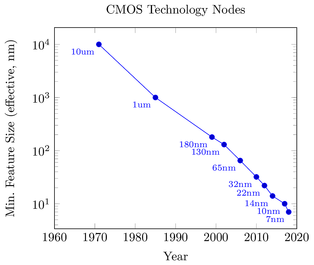
So far, we have learned about classical bulk MOSFET devices, which represent \(L_{\text{min}}\) down to about \(1\mu\)m. In the 1990’s the industry entered the sub-micron era (down to about 180nm), and it became more complicated to scale down device dimensions without losing performance. New manufacturing techniques needed to be developed to pattern devices at this scale.
By 2000, the industry was developing deep sub-micron nodes, reaching dimensions down to 32nm. Deep sub-micron devices required adding new materials and manufacturing steps. Devices were still silicon based, but could include additional layers of non-silicon material to improve performance. After 2014, the most cutting-edge processes migrated to finFET devices, which can attain feature sizes below 30nm, and are forecast to reach 5nm in the near future. With each new technology node, it becomes more expensive to construct fabrication facilities. At the time of this writing, the latest finFET nodes can only be produced by Intel, Samsung and the Taiwan Semiconductor Manufacturing Corporation (TSMC) (see here for a list of present-day foundries with capabilities at advanced technology nodes).
In the classical era from about 1970 through 1995, the MOSFET scaling roadmap was governed by Denard Scaling rules, which prescribed shrinking device dimensions while keeping a constant electric field within the device. Suppose I’m a manufacturer, and starting from my current process, I want to scale it down by a scale factor \(\alpha>1\). Then, to avoid changing the \(\mathcal{E}\)-field, it can be shown that I need to scale my device parameters as follows:
| Parameter | Symbol | Scale |
|---|---|---|
| Gate Length | \(L\) | \(1/\alpha\) |
| Gate Width | \(W\) | \(1/\alpha\) |
| Substrate Doping | \(N_A\) | \(\alpha\) |
| Oxide thickness | \(t_{\text{ox}}\) | \(1/\alpha\) |
| Supply voltage | \(V_{\text{DD}}\) | \(1/\alpha\) |
With these rules, the threshold voltage \({V_{\text{Th}}}\) also tends to drop. As devices got smaller, they tended to run faster by a factor of \(\alpha\), and consumed lower power by a factor of \(\alpha^2\) — a win/win situation. Unfortunately, as the device dimensions shrank into the deep sub-micron regime, these scaling laws stopped working so well.
After about 2005, some problems started to alter the scaling strategies used in the industry, leading to more complex MOSFET structures used today. Dennard’s scaling laws could no longer be used. Some of the major changes are summarized below.
For constant \(\mathcal{E}\)-field scaling, the dielectric oxide thickness \(t_\text{ox}\) has to be reduced proportionally with each process node. But when the dielectric gets too thin, quantum gate tunneling (also called gate leakage) increases exponentially with each new technology node. The benefits of MOSFET circuits rely heavily on zero gate current, so this could seem almost like a show-stopper. To solve this problems, the industry supplemented or replaced the SiO2 dielectric with alternative materials that have a higher relative permittivity, commonly written as \(\epsilon_r\) or \(\kappa\). By using a high-\(\kappa\) dielectric, the gate’s capacitance can be increased without actually scaling \(t_\text{ox}\), and the \(\mathcal{E}\)-field is maintained. Most commonly, the SiO2 layer is implanted with nitrogen, forming an “oxynitride” dielectric. The oxide can also be grown on a polysilicon layer, where it is called “polyoxide”.
The mobility of silicon can be increased by “stretching” the bonds between Si atoms. This is done by depositing a layer of Silicon-Germanium (SiGe), a crystalline alloy in which a fraction of the Si atoms are randomly replaced with Ge atoms. SiGe has a similar lattice structure to Si crystals, but with a larger average inter-atomic distance. When a SiGe is bonded with a Si crystal, the inter-atomic distance increases on the Si side. This creates a big increase in mobility \(\mu\).

When devices are integrated with very small inter-device spacing, there can be cross-device leakage currents exchanged between devices. In order to reduce this, transistors are surrounded by a trench or box to isolate them from their neighbors. The most common isolation is called Shallow Trench Isolation (STI), and some processes offer an enhanced deep-trench isolation (DTI). Trench isolation tends to lower the device’s threshold voltage, which worsens subthreshold leakage current.
Classical bulk MOSFETs are made by directly injecting or diffusing dopants into a Silicon surface. A more complex approach is to deposit MOSFET structures on top of an insulating surface. This has a few advantages: it removes the PN junctions below the Source and Drain terminals, eliminates cross-device leakage paths, and eliminates DIBL. Parasitic junction capacitances are also reduced. SOI devices are also somewhat resistant to errors and damage caused by radiation.
When the channel length is very small, the Drain voltage influences the device’s threshold voltage. As \(V_D\) increases, \({V_{\text{Th}}}\) decreases. In the worst case, DIBL can prevent a device from switching off. In the best case, a lower threshold voltage causes larger subthreshold leakage currents. Since DIBL causes \({V_{\text{Th}}}\) to be signal-dependence, it reduces the MOSFET’s small-signal output resistance (\(r_o\)) and worsens non-linearity in the saturation mode.
The term “mismatch” refers to several types of variations that affect integrated circuits. At the deep sub-micron scale, one of the primary concerns is intra-die mismatch: parametric variation between devices on the same chip. Two nominally identical MOSFETs placed on the same chip will have different \({V_{\text{Th}}}\), \(W\), \(L\), \(\lambda\) and other parameters. In classical bulk MOSFETs, some of these variations could be smoothed out by averaging across large areas. At the nano-scale, the variations are more pronounced. Mismatch is random, and extreme variations can cause a chip to fail. More devices on a chip means more opportunities for failure.
When the \(\mathcal{E}\)-field strength increases beyond a critical level, electron velocity reaches a maximum value. Beyond this level, the velocity is no longer proportional to \(\mathcal{E}\) and is said to be saturated. To see why this is a problem for sub-micron devices, suppose there is a 1V difference between the Drain and Source terminals. Since the \(\mathcal{E}\)-field has units of V/cm, in a 1\(\mu\)m device this causes \(\mathcal{E}\sim 10^4\) V/cm. In Silicon, velocity saturation starts occurs at \(\mathcal{E}\sim 10^5\) V/cm, so its effects can be particularly seen for dimensions below 100nm. The main consequence of velocity saturation is a reduction in transconductance (\(g_m\)). Since the current becomes relatively constant, there is also an increased output resistance (\(r_o\)). Strained Silicon tends to improve the saturation velocity.
The area occupied by MOSFET devices has decreased much faster than the device currents. As a result, the current density has increased over time, leading to a rising heat density in modern integrated circuits. High chip temperatures alter device parameters, can degrade performance, and cause damage to the device. There is also a risk of thermal runaway, since some chips draw higher currents at higher temperatures, leading to a positive feedback effect. Self-heating tends to be worsened by strained silicon technology, so thermal management has become an important aspect of modern CPUs and other complex chips.
Occasionally, high-velocity electrons called hot carriers penetrate into the gate insulation of NMOS devices and get stuck there. These are called oxide traps. They accumulate over time in proportion to the chip’s activity. Their effect is to steadily lower the threshold voltage until the device can no longer effectively switch off. At that point, the chip will fail.
NBTI is the counterpart of hot-carrier injection affecting PMOS devices. The physics is different but the effect is similar.
The industry’s latest answer to sub-micron challenges is the FinFET, so called because the channel is made from a nano-scale “fin” of Silicon. The gate is deposited all the way around the fin, as shown in the figure below. In a sense, the Gate width W corresponds to the fin’s perimeter. So even though the fin is only 10nm across, the gate could cover more than 60nm.

The FinFET is often described as a Multiple-Gate FET (MuGFET). Each side of the fin can operate as a gate. In the illustration above, the four gates are labeled \(g_1\), \(g_2\), and so on. Some technologies are able to get a thin oxide only along \(g_1\) and \(g_2\), so these are called double-gate FinFETs. A triple-gate FinFET also has a thin oxide along \(g_3\). A Gate All Around FET (GAAFET) or quad-gate FinFET is able to achieve control on all four surfaces.
By draping the gate around a narrow fin, several nano-scale problems are resolved. The channel is strongly controlled by the gate, and Drain effects (like DIBL) are suppressed. Channel Length Modulation is also reduced, so FinFETs can have a fairly high output resistance. Strained Silicon can be used to improve mobility, and \(\mathcal{E}\)-fields have been able to stay below the level for velocity saturation. Subthreshold leakage currents are quite low, so the \(I_{\text{ON}}/I_{\text{OFF}}\) ratio is better than in deep sub-micron planar MOSFETs. SOI processes are also used, further reducing leakage currents. Matching is also reportedly very good in FinFET processes.
The fins used in FinFET processes are patterned with a fixed size. This means every FinFET has the same width \(W\). To make a device with larger width, a parallel combination of \(M\) FinFETs can be connected in a fairly small area. In this approach, \(M\) is called the multiplier parameter, and the total effective device width is \(MW\). Since multipliers are commonly used, FinFET chips tend to look like waffles.