
READ operation. The controller WRITEs a command on SDI, and the peripheral responds with requested data on SDO.Many SPI devices support two-way communication using both SDO (serial data out) and SDI (serial data in) wires. The signalling is initiated using the CS_n wire, and timing is controlled using the SCLK wire. Since there is only one CS_n wire, a bi-directional SPI peripheral has no idea whether the operation is READ or WRITE.
To solve this problem, most peripherals operate in WRITE mode by default, watching for a command on the SDI wire. The device defines a set of command codes that can be issued via the SDI interface. All bus transactions begin with a command code, followed by either a READ from SDO or a WRITE on SDI.
On the controller side, in order to READ data from the peripheral the controller must first WRITE the appropriate command code onto SDI, then the peripheral immediately responds with the requested data on SDO.
spi_register PeripheralTo demonstrate a cmd/read/write SPI interface, we will use a simple spi_register peripheral design with these specifications:
We will use distinct terms for SPI bus operations as opposed to internal peripheral command codes. Here is a key to the terminology:
READ – controller sends a command on SDI, the peripheral sends data on SDOWRITE – controller sends a command on SDI, the controller sends data on SDIGET – peripheral detects command 50h, transmits register data on SDIPUT – peripheral detects command 46h, overwrites register data from SDOWe will use the terms READ/WRITE to describe timing specifications for the SPI signals, and the terms GET/PUT refer to the peripheral’s internal logic.
posedge (controller) and negedge (peripheral)In order for the controller and peripheral to synchronize reliably, the peripheral is usually synchronized to the negative edge of SCLK. If the controller is synchronized to the positive edge, then some of the state machine logic is simplified. This two-phase strategy is depicted in the timing diagram for a READ operation shown below.
In the above diagram, all of the controller actions occur on the positive SCLK edges (gray lines). So CS_n and SDI change with the positive edges. The peripheral “sees” the SDI values on the negative SCLK edges (blue lines). For each bit of the command code (shaded in red), SDI is stable at the time the peripheral “sees” it.
When the peripheral answers on the SDO wire, the signal changes with the negative edges of SCLK. The controller “sees” the SDO values on the positive SCLK edges, so the signal is stable at the time it is sensed by the controller.
The timing for a WRITE operation is similar, shown in the diagram below. For the WRITE operation, all SDI changes occur on the positive edges of SCLK, and the values are sensed by the peripheral on the negative edges.

In this assignment, you will create an SPI interface for a single-word 16-bit register. The spi_register “peripheral” will reside inside the FPGA, simulating an external device. The user (you) supplies input data using the sw inputs on the Basys3 board, and output data is displayed on the board’s led lights. To write data into the spi_register, the user presses a button designated as the wr_btn, causing the controller to write bits from sw into the spi_register. When the user presses rd_btn, the controller reads bits from the spi_register and displays them on led. A block diagram for this system is shown below.

The state transition diagram shown below is based on the simpleSPI READ interface that we developed for the PmodALS project. This version of the diagram is referred to as “high-level” because it does not show every precise operation, and some operations are described in normal English to clarify the behavior.

This FSM design is very similar to the read-only interface we studied previously, with a few key differences:
wr and rdCMD state to write the cmd_code bitsREAD and WRITE states occur after the CMD stateWe will trigger the GET and PUT commands using buttons on the Basys3 board. Each buttons requires a debouncer module. We will modify the debouncer so that it implements a rd/wr/done handshaking protocol with simpleSPI. The behavior should be like this:
debouncer waits in state 0btn is pressed, debouncer moves to state 1, starts the tcounterbtn bounces to 0, then debouncer resets to state 0btn is sustained until the counter event t, then debouncer moves to state 2 and raises the command signal, either rd or wr.rd/wr stays high until simpleSPI answers with the done signal; when done goes high, debouncer resets to state 0 and lowers the command signal.The altered state machine looks like this:
     case (state)
       0: // WAIT FOR PRESS
         begin
        if (btn) begin
           clear <= 0;
           state <= 1;
        end
        else begin
           clear <= 1;

        end
         end // case: 0
       1: // PRESS
         begin
            // BUTTON SUSTAINED:
        if (t && btn) begin
           state <= 2;
           btn_db <= 1;
        end
        // BOUNCE:
        else if (!btn && !t) begin
           state <= 0;
           clear <= 1;
        end
         end // case: 1
       2: // WAIT FOR DONE
         begin
        if (done) begin
           btn_db <= 0;
           state <= 0;
           clear <= 1;
        end
         end
     endcase // case (state)
Copy your debouncer.v Verilog source from the previous assignment into src/ and make the changes needed to implement the state machine described here.
Copy your simpleSPI design from the previous assignment, and modify it to enable WRITE operations as follows:
  input             wr,
  input         rd,
  input      [15:0] d_in,
  output reg [15:0] d_out,
output reg doneSDI: output reg CS_n,
output reg SCLK,
output reg SDI, // from controller to peripheral
input SDO // from peripheral to controllerlocalparam to define command codes: localparam GET_CODE = 8'h50;
localparam PUT_CODE = 8'h46;bit_index declaration to ensure it can support values up to 15.state declaration to ensure it can support all the unique state numbers.reg named cmd_code to contain the selected command.initial block to initialize any new signals.localparam to define state values for RST, INIT, and all the other states.d_ready signal since we will now use done for handshaking on both wr and rd commands.CMD, READ and WRITE states based on the high-level state diagram.top ModuleCreate a top module with the features listed below.
wire signals:
CS_n, SCLK, SDI, and SDOwr, rd, and doneassign a rst_n signal derived from rstsimpleSPI module and name the instance SPI_iface
wires to SPI_ifacewires wr, rd, and donesw to port d_in, and led to port d_outspi_register module with instance name memoryModel, using the port definitions declared in src/spi_register.v.
SPI_iface and memoryModeldebouncers for wr_btn and rd_btn, with instances named wdb and rdb respectively.
wr and rd to the btn_db outputs on their respective debouncer modulesA testbench is provided in src/testbench.v. This testbench simulates random button presses on rd_btn and wr_btn, with random values generated on sw. causing it to perform GET and PUT operations at random times. A VCD file is produced, and a text output is generated as in previous assignments.
If your design is correct from the start (an unlikely event), then your output should resemble the text below. SDI values are printed on the negedge of SCLK, and SDO values are printed on the posedge. When a PUT/GET operation begins, the testbench prints an information message “Starting GET” or “Starting PUT”. The next 8 lines should show the command bits on SDI (bolded below). For a GET operation, the next 16 lines should show the register bits (initially ABCDh). For a PUT operation, they should show the bits from d_in.
Starting GET
negedge sw: 90a8 SDI: 0   posedge  SDO: 1 led: 0000 (0000000000000000)
negedge sw: 90a8 SDI: 1   posedge  SDO: 1 led: 0000 (0000000000000000)
negedge sw: 90a8 SDI: 0   posedge  SDO: 1 led: 0000 (0000000000000000)
negedge sw: 90a8 SDI: 1   posedge  SDO: 1 led: 0000 (0000000000000000)
negedge sw: 90a8 SDI: 0   posedge  SDO: 1 led: 0000 (0000000000000000)
negedge sw: 90a8 SDI: 0   posedge  SDO: 1 led: 0000 (0000000000000000)
negedge sw: 90a8 SDI: 0   posedge  SDO: 1 led: 0000 (0000000000000000)
negedge sw: 90a8 SDI: 0   posedge  SDO: 1 led: 8000 (1000000000000000)
negedge sw: 90a8 SDI: 0   posedge  SDO: 0 led: 8000 (1000000000000000)
negedge sw: 90a8 SDI: 0   posedge  SDO: 1 led: a000 (1010000000000000)
negedge sw: 90a8 SDI: 0   posedge  SDO: 0 led: a000 (1010000000000000)
negedge sw: 90a8 SDI: 0   posedge  SDO: 1 led: a800 (1010100000000000)
negedge sw: 90a8 SDI: 0   posedge  SDO: 0 led: a800 (1010100000000000)
negedge sw: 90a8 SDI: 0   posedge  SDO: 1 led: aa00 (1010101000000000)
negedge sw: 90a8 SDI: 0   posedge  SDO: 1 led: ab00 (1010101100000000)
negedge sw: 90a8 SDI: 0   posedge  SDO: 1 led: ab80 (1010101110000000)
negedge sw: 90a8 SDI: 0   posedge  SDO: 1 led: abc0 (1010101111000000)
negedge sw: 90a8 SDI: 0   posedge  SDO: 0 led: abc0 (1010101111000000)
negedge sw: 90a8 SDI: 0   posedge  SDO: 0 led: abc0 (1010101111000000)
negedge sw: 90a8 SDI: 0   posedge  SDO: 1 led: abc8 (1010101111001000)
negedge sw: 90a8 SDI: 0   posedge  SDO: 1 led: abcc (1010101111001100)
negedge sw: 90a8 SDI: 0   posedge  SDO: 0 led: abcc (1010101111001100)
negedge sw: 90a8 SDI: 0   posedge  SDO: 1 led: abcd (1010101111001101)
negedge sw: 90a8 SDI: 0   posedge  SDO: 1 led: abcd (1010101111001101)
Completed GET with data abcd
For a PUT operation, the SDO signal stays constant and all the data appears on SDI:
Starting PUT with data 7b69
negedge sw: 7b69 SDI: 0  SDO: 1 led: abcd (1010101111001101)
negedge sw: 7b69 SDI: 1  SDO: 1 led: abcd (1010101111001101)
negedge sw: 7b69 SDI: 0  SDO: 1 led: abcd (1010101111001101)
negedge sw: 7b69 SDI: 0  SDO: 1 led: abcd (1010101111001101)
negedge sw: 7b69 SDI: 0  SDO: 1 led: abcd (1010101111001101)
negedge sw: 7b69 SDI: 1  SDO: 1 led: abcd (1010101111001101)
negedge sw: 7b69 SDI: 1  SDO: 1 led: abcd (1010101111001101)
negedge sw: 7b69 SDI: 0  SDO: 1 led: abcd (1010101111001101)
negedge sw: 7b69 SDI: 0  SDO: 1 led: abcd (1010101111001101)
negedge sw: 7b69 SDI: 1  SDO: 1 led: abcd (1010101111001101)
negedge sw: 7b69 SDI: 1  SDO: 1 led: abcd (1010101111001101)
negedge sw: 7b69 SDI: 1  SDO: 1 led: abcd (1010101111001101)
negedge sw: 7b69 SDI: 1  SDO: 1 led: abcd (1010101111001101)
negedge sw: 7b69 SDI: 0  SDO: 1 led: abcd (1010101111001101)
negedge sw: 7b69 SDI: 1  SDO: 1 led: abcd (1010101111001101)
negedge sw: 7b69 SDI: 1  SDO: 1 led: abcd (1010101111001101)
negedge sw: 7b69 SDI: 0  SDO: 1 led: abcd (1010101111001101)
negedge sw: 7b69 SDI: 1  SDO: 1 led: abcd (1010101111001101)
negedge sw: 7b69 SDI: 1  SDO: 1 led: abcd (1010101111001101)
negedge sw: 7b69 SDI: 0  SDO: 1 led: abcd (1010101111001101)
negedge sw: 7b69 SDI: 1  SDO: 1 led: abcd (1010101111001101)
negedge sw: 7b69 SDI: 0  SDO: 1 led: abcd (1010101111001101)
negedge sw: 7b69 SDI: 0  SDO: 1 led: abcd (1010101111001101)
negedge sw: 7b69 SDI: 1  SDO: 1 led: abcd (1010101111001101)
Completed PUT with data 7b69
Following a PUT operation, the subsequent GET operation should return the same data:
Starting PUT with data 7b69

...

Completed PUT with data 7b69
Starting GET

...

Completed GET with data 7b69
If your initial simulation result doesn’t have the correct behavior, you should diagnose the problem using a graphical waveform viewer, either use gtkwave to view the VCD file, or run the simulation using make gui. Closely inspect the timing for GET and PUT operations, paying careful attention to the positive and negative SCLK edges, and the state of your simpleSPI interface.
As your designs become increasingly complex, you will need to develop skills and habits to systematically diagnose design errors. For any design, you should contemplate possible test failures and imagine their possible causes. Below are some common examples.
testbench.
CS_n goes LOW, triggered by
simpleSPI entering CMD state, triggered bysimpleSPI receives rd or wr while in WAIT state, preceded by
debouncer modules acting on rd_btn or wr_btn, dependent on…simpleSPI starting in RST then INIT states, triggered by…This listing is the beginning of a Fishbone Diagram or Ishikawa Diagram, which is a systematic method to diagnose the root causes of a problem. An example diagram is shown below. When analyzing the problem, we trace back along the branches, first checking the most “obvious” or top-level items on the right, then exploring the deeper items toward the left.

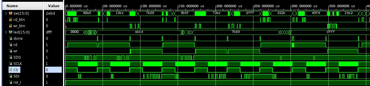
Let’s study an example failure. After completing the simpleSPI, top and debouncer modules, the testbench simulation runs with no output. The simulation ran with no error messages, so the problem is not due to a syntax error. At this point, we should inspect the signal waveforms using either make gui or gtkwave.
First, we check the top-level signals, clk and rst_n.
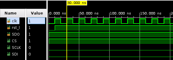
The top-level signals look good, so next we check SCLK.
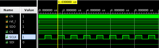
SCLK looks good, so next we’ll investigate the handshake signals:
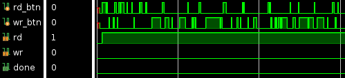
Here we can see that the buttons rd_btn and wr_btn are being “pressed”, and the system is stuck in a rd request, but the operation never starts.
Next we’ll examine the state register in simpleSPI, along with its dependencies (the dependencies are the signals used for any edge conditions in the state graph).
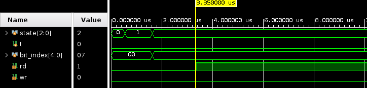
Here we notice that simpleSPI arrives in state 2 (WAIT), but does not go any further. Judging from the state transition diagram, in order to reach state 3 the condition is t && (rd || wr). From the signal plot, we can see that rd goes high but t never does. This points to the tcounter as the problem.
Now examining all the signals related to the tcounter:
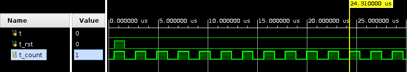
In this signal plot we notice something truly odd: the tcount is supposed to count up to ten, but instead it just toggles between 0 and 1. Since this is unexpected behavior, we examine the source code related to tcount:
   //-----------------------------------------
   // Alarm Timer Process
   //-----------------------------------------
   always @(posedge SCLK) begin
      if (t_rst) begin
     t       <= 0;
     t_count <= 0;
      end
      else begin
     if (t_count > 10) begin
        t <= 1;
     end
     else begin
        t_count <= t_count + 1;
     end
      end
   end
   //-----------------------------------------
After studying each line and conditional statement, the code looks correct. The problem must be in some other section of the source code. There are two possibilities:
t_count elsewhere in the same module.To track it down, we can do a text search for every occurrence of t_count. These are all the other lines that involve t_count (I cut out all the other signals so we can focus just on t_count):
   reg        t_count;    // timer count

   initial begin
      t_count    = 0;
   end
There’s the mistake: t_count is declared as a reg, which has only one bit by default. In order for t_count to count up to 10, it needs at least 4 bits. We fix the mistake:
reg [3:0] t_count; // timer count (4 bits)
Now repeating the simulation, we see the expected testbench output and the signal patterns look more correct:
Once the testbench simulation is verified to be correct, run make implement to create the bitstream, and program it onto the Basys3. The button mappings are:
btnU: GETbtnD: PUTbtnC: rstAfter programming, perform a GET operation and verify that you see the value ABCDh on the LEDs. Then record a short video showing LEDs initially at led = 0000h, with the switches set to sw = 1071h. Press PUT then GET to show that 1071h appears on the LEDs. Turn in the video on Canvas.
Turn in your work using git:
git add src/*.v *.v *.rpt *.txt *.tcl *.bit *.xdc *.vcd
git commit . -m "Complete"
git push origin master
Indicate on Canvas that your assignment is done.